

Embedded Channels, Embedded Waveguide And Methods Of Manufacturing And Using The Same
a technology of embedded waveguides and embedded channels, which is applied in the direction of glass blowing apparatus, glass shaping apparatus, instruments, etc., can solve the problems of inability to manufacture and use silicon processes, inability to meet the speed demands of micro-electronic processors, and inability to meet the speed requirements of micro-electronic processors
- Summary
- Abstract
- Description
- Claims
- Application Information
AI Technical Summary
Benefits of technology
Problems solved by technology
Method used
Image

Examples
example 1
Horizontal or Lateral Waveguides
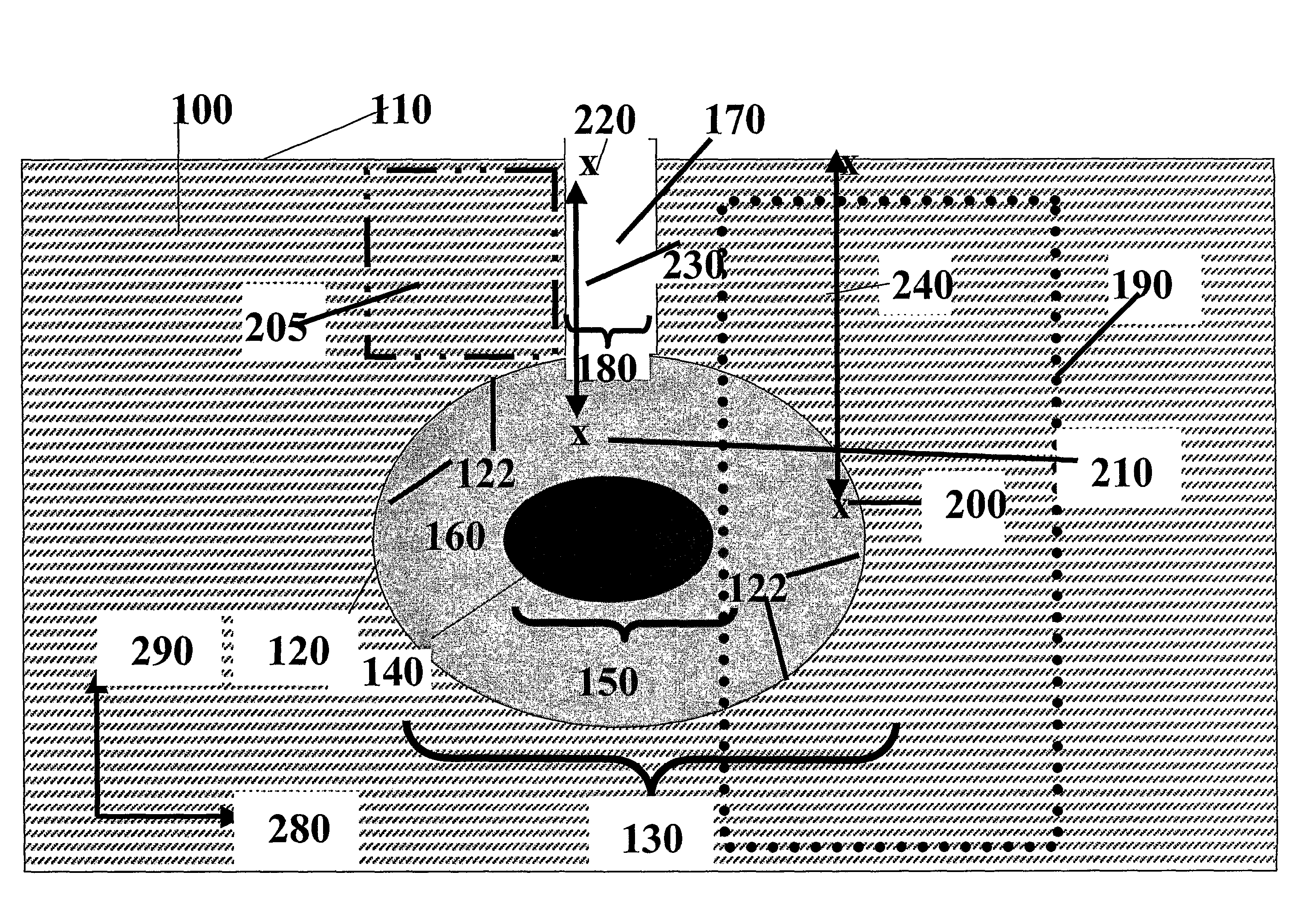
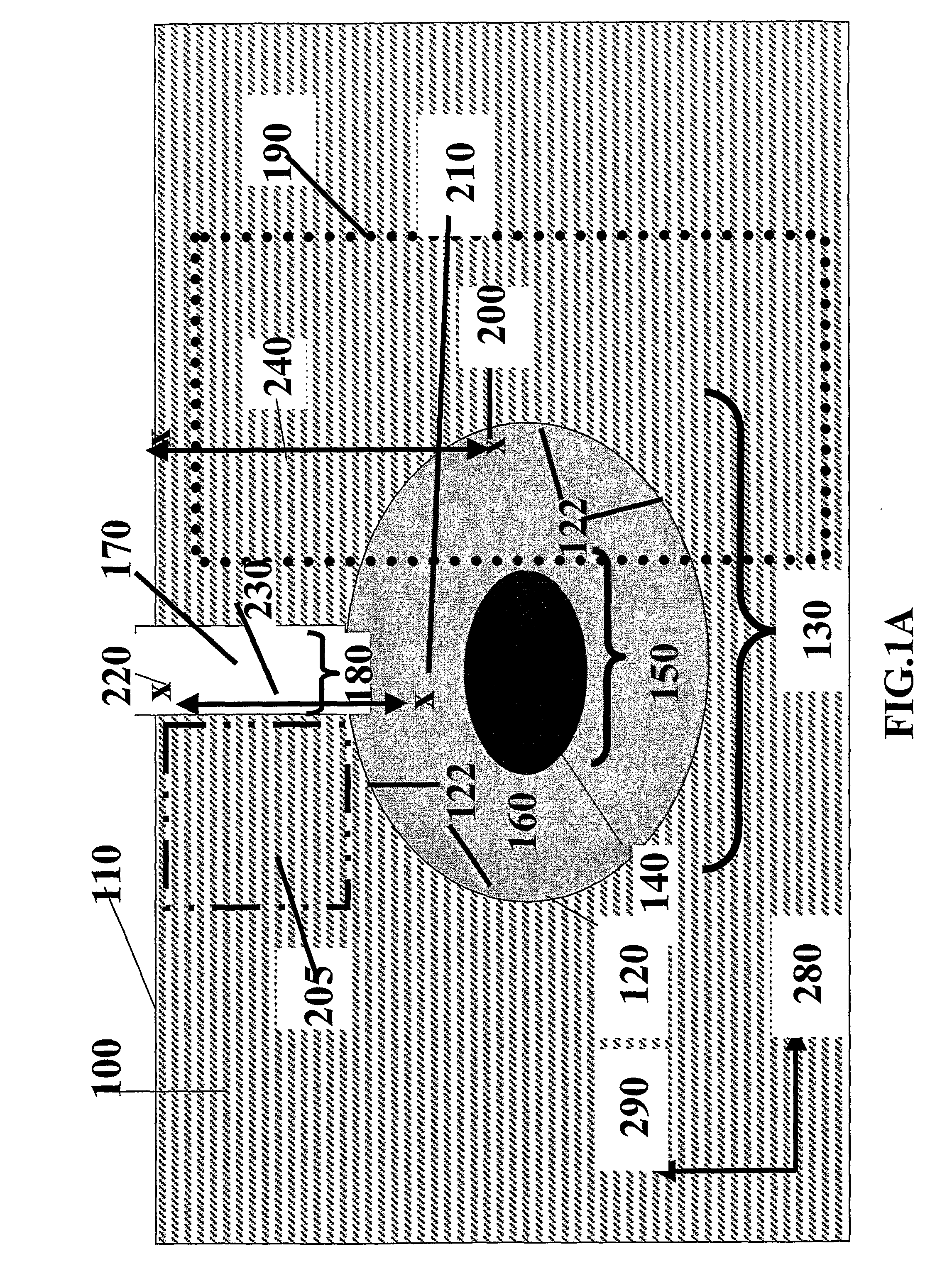
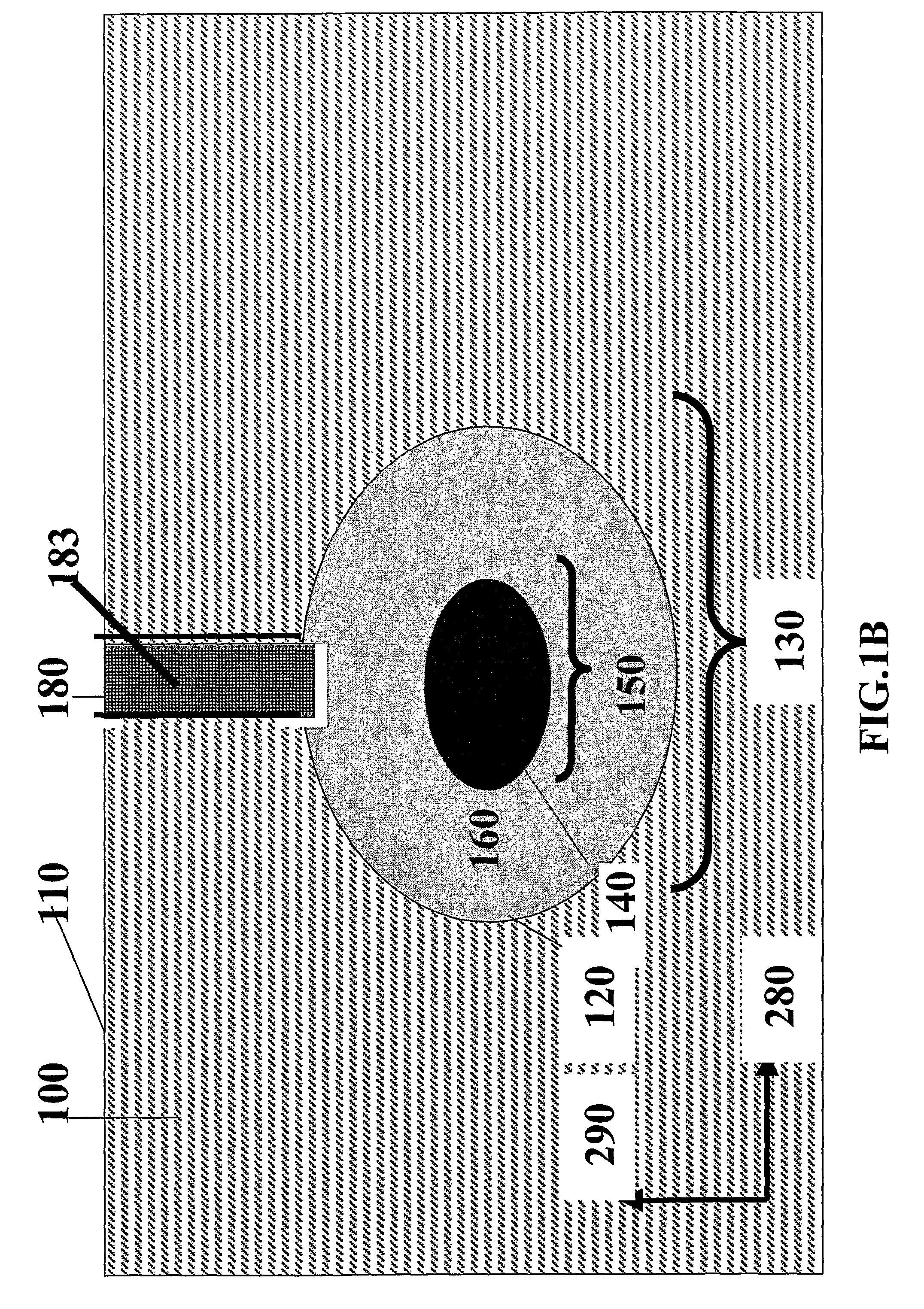
[0219]FIG. 2 describes and depicts an exemplary process for the creation of horizontal tubular waveguides embedded in silicon, though it is stressed that the waveguides and channels disclosed herein may be manufactured using processes other than those of FIG.
[0220]As seen, the first step here is the creation of a protective layer, in our case the layer was silicon dioxide, but silicon nitride may be even better. The method preferred here was the placing of the silicon wafer in a furnace within an ambient containing Oxygen and water (We used only dry oxidation—only O2 gas (0.99%), but wet oxidation method (with water vapor) is applicable, as well.) at partial pressures of a few hundred milliTorr (100-300 mTorr) and temperature of 1050° C. for a few hours (3-8 hours). Next, openings are created by standard photolithography process in a photo-resist layer. Next, two dry-etching processes are described: one of them is to etch the Silicon Dioxide layer and...
example 2
Deep Buried Horizontal Closed Round Hollow Channels in Silicon (Tubes)
[0223]The following describes an extension of the process detailed above and its purpose is making of a spherical cross-section buried closed and long hollow tubes. The tube scan be applied for fabrication of the optical waveguides, thermo-stabilization, or cooling micro system, micro chemical laboratory (micro-mixer), etc.
[0224]FIG. 3 shows schematically the process.
[0225]As seen in FIG. 3, steps 1-4 are identical to process A described above in Example 1, except that in the last step (4) one aims to reach deeper depths according to the specific application in mind. In the steps following, a further oxidation process takes place following an isotropic etching step aiming to etch the bottom oxide layer of the generated hole. Step 8 is an isotropic etch of the silicon bulk material, and the two last steps are dry and wet oxidations with the purpose of conditioning the tube's wall and sealing the tube.
[0226]Step 10 ...
example 3
Vertical Tubular Waveguides in Silicon
[0232]The idea here is to present a method for directing light from one side of a silicon wafer to the opposite one. Silicon material is opaque for light having wavelength smaller than 1.1 mm. For light of longer wavelength silicon is transparent and possesses a rather high refractive index (n˜3.5). The method presented here is able to function for light both smaller and larger than 1.1 mm. Its transparency depends only on the transparency of the materials comprising the waveguides. The principle and method are similar to those described in the preceding sections. FIG. 4 shows the etched holes in plane and cross-section views. The hole (or traverse channel) of FIG. 4 has a width 130B.
[0233]The fabrication includes the steps:
[0234]1. Photolithography;
[0235]2. Etching of the silicon by dry anisotropic method (ICP-IRE technology);
[0236]3. Dry or wet oxidization of the etched channel.
[0237]For rather thick wafers like those customarily used in semic...
PUM
| Property | Measurement | Unit |
|---|---|---|
| Fraction | aaaaa | aaaaa |
| Thickness | aaaaa | aaaaa |
| Structure | aaaaa | aaaaa |
Abstract
Description
Claims
Application Information