Photodetector and production method thereof
a technology of photodetector and production method, which is applied in the field of photodetector, can solve the problems of increasing dark current and affecting crystal quality, and achieve the effect of suppressing dark curren
- Summary
- Abstract
- Description
- Claims
- Application Information
AI Technical Summary
Benefits of technology
Problems solved by technology
Method used
Image
Examples
first embodiment
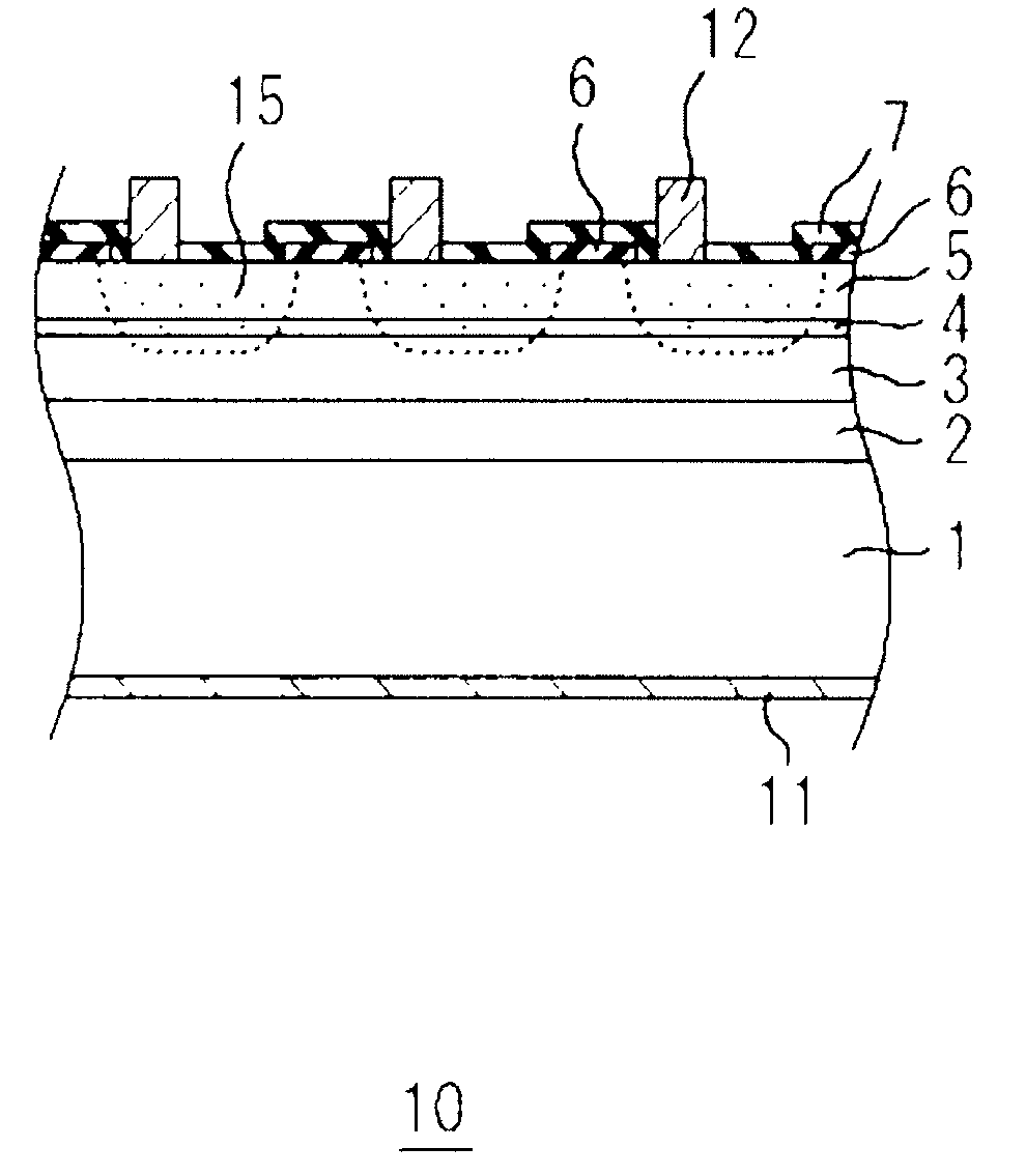
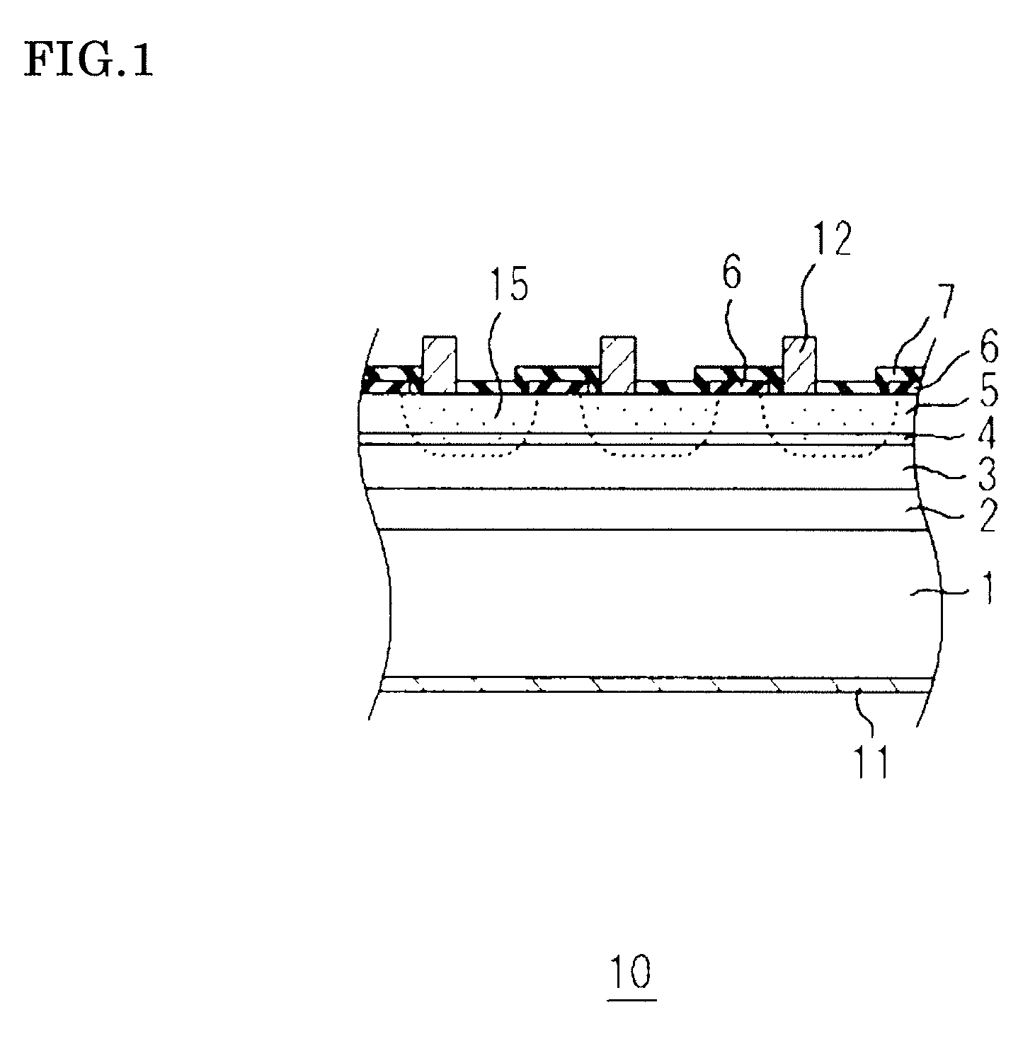
[0064]Embodiments of the present invention described above are explained below. First embodiment explains the results of the measurement of dark current performed on Example A and Comparative example B. Specimens of the two examples each had a laminated structure formed through the MBE method without being subjected to an annealing operation for dehydrogenation. As shown in FIG. 1, Example A had a laminated structure in which the InGaAs buffer layer 4 was placed between the GaInNAs absorption layer 3 and the InP window layer 5. On the other hand, as shown in FIG. 5, the photodiode 110 of Comparative example B was formed by epitaxially growing the InP window layer 105 directly on the GaInNAs absorption layer 103. Both specimens had the same structure except for the portions described above. The GaInNAs absorption layers 3 and 103 each had an N content of 1.0 at % in the V-group atoms (in the expression Ga1-xInxNyAs1-y, the N content is y=0.01) and a peak wavelength of 1.8 μm in photo...
second embodiment
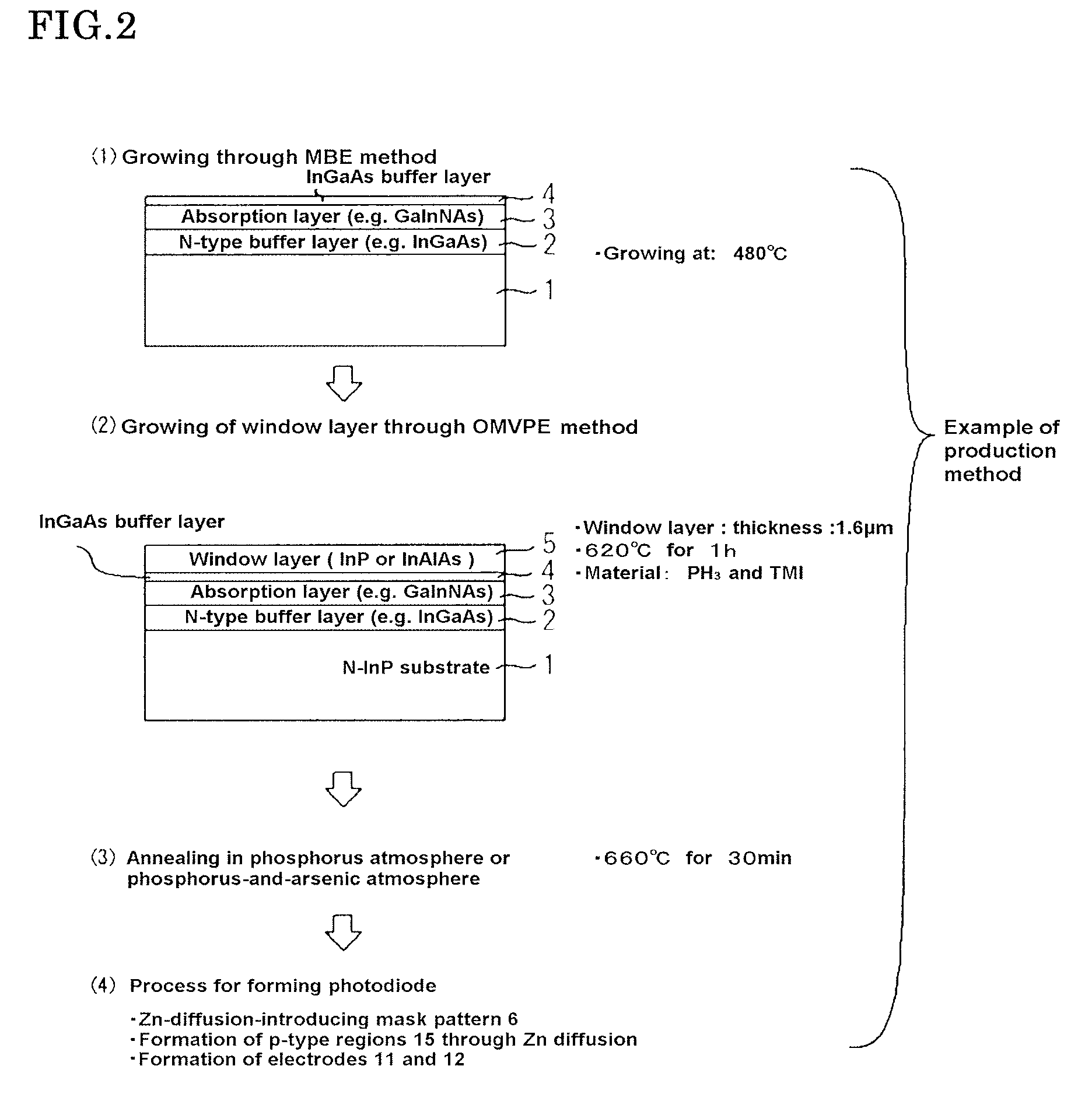
[0067]Second embodiment explains the results of the measurement of dark current performed on Examples C1 to C4. Although Examples C1 to C4 each have a laminated structure according to the present invention, their production methods are different from one another as shown below.[0068]Example C1: On the InP substrate 1, the InGaAs buffer layer 2, the GaInNAs absorption layer 3, the InGaAs buffer layer 4, and the InP window layer 5 were all grown successively through the OMVPE method. No annealing operation was performed thereafter.[0069]Example C2: As with Example C1, a laminated structure was formed by using the OMVPE method for forming all the layers. Subsequently, an annealing operation was performed at 660° C. for 30 minutes.[0070]Example C3: On the InP substrate 1, the InGaAs buffer layer 2, the GaInNAs absorption layer 3, the InGaAs buffer layer 4, and the InP window layer 5 were all grown successively through the MBE method. Subsequently, an annealing operation was performed at...
PUM
 Abstract
Description
Claims
Application Information


