Comparator circuit

a comparator circuit and circuit technology, applied in pulse manipulation, pulse technique, instruments, etc., can solve the problems of slow average voltage rise, long time to obtain binarized data, and average voltage vref cannot adapt to it quickly

Inactive Publication Date: 2009-01-01
KK TOSHIBA
View PDF9 Cites 6 Cited by
  • Summary
  • Abstract
  • Description
  • Claims
  • Application Information

AI Technical Summary

Benefits of technology

[0014]An aspect of the present invention is, for example, a comparator circuit including a comparator configured to compare an input signal voltage with a reference voltage obtained by smoothing the input signal by use of a resistor and a capacitor, and output a result of the comparison, a discharge circuit configured to compare a first addition signal which is obtained by adding a positive first voltage to the input signal voltage, with the reference voltage, and discharge the capacitor when the first addition signal is lower than the reference voltage, and a charge circuit configured to compare a second addition signal which is obtained by adding a negative second voltage to the input signal voltage, with the reference voltage, and charge the capacitor when the second addition signal is higher than the reference voltage.

Problems solved by technology

For this reason, the capacitance of the capacitor becomes large, time for charging and discharging becomes long, the rise of the average voltage becomes slow, and hence it takes a long time to obtain the binarized data.
Therefore, when the input signal voltage Vin varies, the average voltage Vref cannot adapt to it rapidly, due to the time constant of the primary low-pass filter including the resistor and the capacitor.
However, it is impossible to set arbitrarily a voltage at which charging / discharging is started, and therefore this voltage is fixed at ±VF.
Further, the forward voltage VF of a diode is about as large as 0.6 V, and it has been difficult to adapt to the reduction of the signal amplitude resulting from the recent trend toward low power-supply voltages.
), and it has been difficult to obtain high reliability.
In this method that involves using the primary low-pass filter, if the cut-off frequency is set at a value sufficiently lower than the signal frequency to prevent the attenuation of the FSK signal or the ASK signal, the rise of the average voltage becomes slow and it takes a long time before the binarization is completed.
For this reason, when the method is applied to a system that operates on battery, the consumption of the battery becomes severe, the battery needs to be replaced frequently, and hence the usability of the system becomes poor.

Method used


Image

  • Comparator circuit
  • Comparator circuit
  • Comparator circuit

Examples


first embodiment

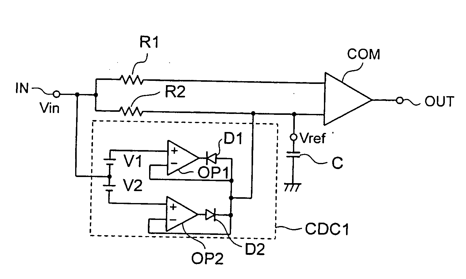
[0057]FIG. 2 shows the configuration of a comparator circuit in the first embodiment.

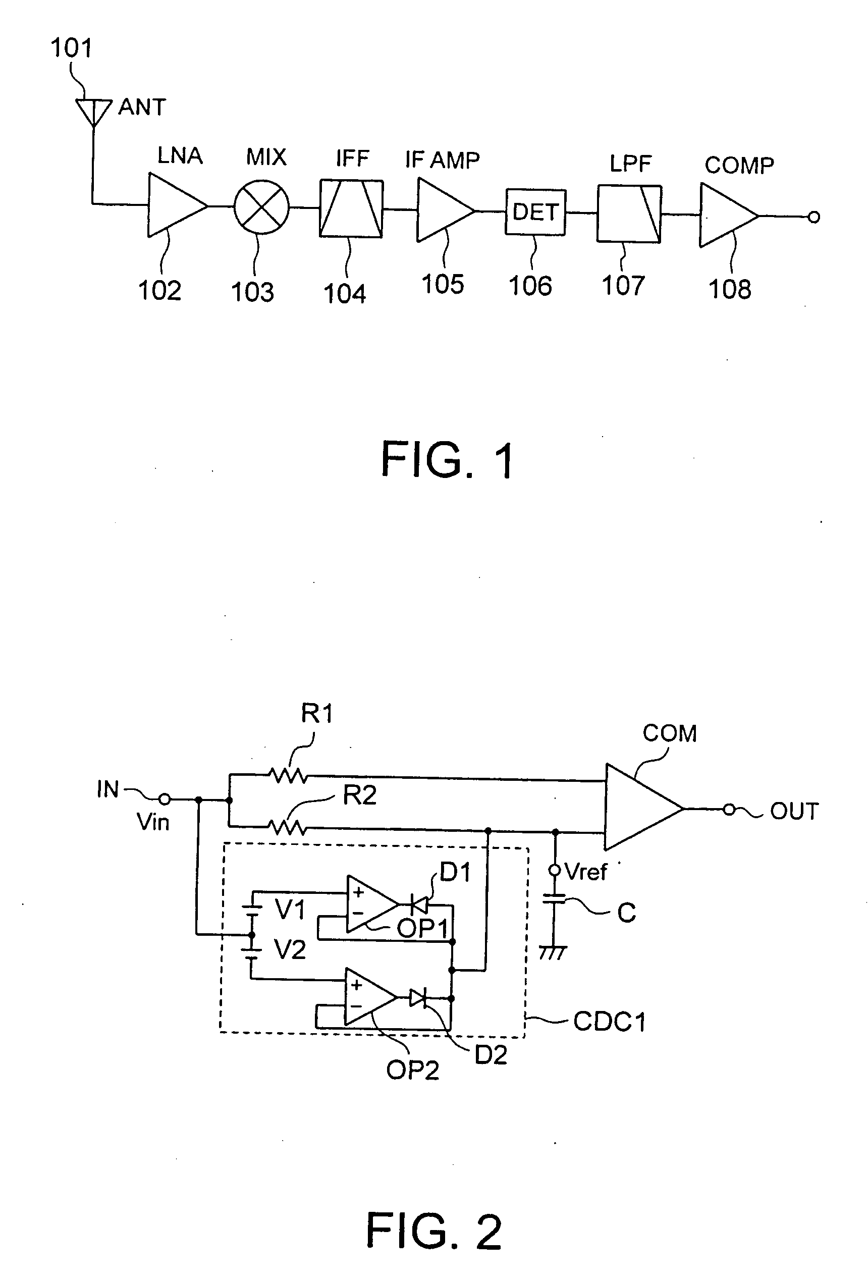
[0058]In the FM detection by the above FSK receiving circuit, the DC voltage of a detection output varies in proportion to the input frequency. Therefore, the DC voltage varies when there happens a change from a no-signal condition to a condition in which a signal is present, and the comparator circuit 108 is required to adapt to this change rapidly.

[0059]This comparator circuit 108 has a comparator COM whose first and second input terminals are connected to resistors R1 and R2 respectively, and an input signal voltage Vin is input to the first and second input terminals via an input terminal IN.

[0060]A capacitor C is connected between the second input terminal and a ground terminal. An average voltage Vref which is used for comparison is generated in the second input terminal by a low-pass filter including the resistor R2 and the capacitor C. A charge / discharge circuit CDC1 is provided to rapidly c...

second embodiment

[0081]A comparator circuit in the second embodiment will be described with reference to FIG. 6 showing the configuration of the comparator circuit.

[0082]The second embodiment differs from the above-described first embodiment in that a gain-variable type operational amplifier OP3 is connected in series between the input terminal IN, and the connection point of the resistors R1 and R2 in the first embodiment.

[0083]The level of an input signal voltage Vin1 input from the input terminal IN is changed by the gain-variable type operational amplifier OP3, and the input signal voltage Vin1 is output to the succeeding stage as an input signal Vin2.

[0084]According to the second embodiment, even in a case where an input signal voltage Vin1 given by the low-pass filter 107 in the preceding stage shown in FIG. 1 fluctuates and varies, an adjustment is made so that the relationship 2×V1 (or V2)=Vin2 (p-p) holds by changing the level by use of the gain-variable type operational amplifier OP3, ther...

third embodiment

[0098]The configuration of a comparator according to the third embodiment is shown in FIG. 11. In the above-described second embodiment, the level of the input signal voltage Vin is made variable, thereby an adjustment is made so that the relationship 2×V1 (or V2)=Vin2 (p-p) holds.

[0099]In contrast to this, in the third embodiment, the charge / discharge start voltage is made variable in the stage when the charge / discharge start voltage is input to the operational amplifiers OP1, OP2 in a charge / discharge circuit CDC3, thereby voltages V1a, V1b are adjusted as variable voltages so that the relationship 2×V1a (or V1b)=Vin2 (p-p) holds.

[0100]Other elements that are the same as in the above-described first embodiment are identified by the same reference numerals as in the first embodiment, and the descriptions of these elements are omitted.


PUM


Abstract

A comparator circuit according to an embodiment of the present invention includes a comparator configured to compare an input signal voltage with a reference voltage obtained by smoothing the input signal by use of a resistor and a capacitor, and output a result of the comparison, a discharge circuit configured to compare a first addition signal which is obtained by adding a positive first voltage to the input signal voltage, with the reference voltage, and discharge the capacitor when the first addition signal is lower than the reference voltage, and a charge circuit configured to compare a second addition signal which is obtained by adding a negative second voltage to the input signal voltage, with the reference voltage, and charge the capacitor when the second addition signal is higher than the reference voltage.

Description

CROSS REFERENCE TO RELATED APPLICATION[0001]This application is based upon and claims the benefit of priority from the prior Japanese Patent Application No. 2007-171821, filed on Jun. 29, 2007 and the prior Japanese Patent Application No. 2008-94599, filed on Apr. 1, 2008, the entire contents of which are incorporated herein by reference.BACKGROUND OF THE INVENTION[0002]1. Field of the Invention[0003]The present invention relates to a comparator circuit, for example, a comparator circuit for an FSK (frequency shift keying) demodulation circuit, and a comparator circuit suited to binarizing an ASK (amplitude shift keying) signal demodulated using an RSSI (received signal strength indicator).[0004]2. Background Art[0005]In demodulating an FSK signal, it is common practice to remove a signal component included in the FSK signal to extract a DC component, deal with the extracted component as an average voltage of the FSK signal, and compare this voltage as a threshold voltage with the F...

Claims


Application Information

Patent Timeline
Patent Type & Authority Applications(United States)
IPC IPC(8): G11C27/02
CPCH03K5/082H04L27/1563H04L27/06H04L25/061
Inventor YAMAMOTO, TATSUYASUZUKI, TSUNEOMAEDA, YUUSUKEHONMA, SOUICHI
Owner KK TOSHIBA
Why Eureka
Try Eureka