

Process for forming cobalt and cobalt silicide materials in tungsten contact applications
- Summary
- Abstract
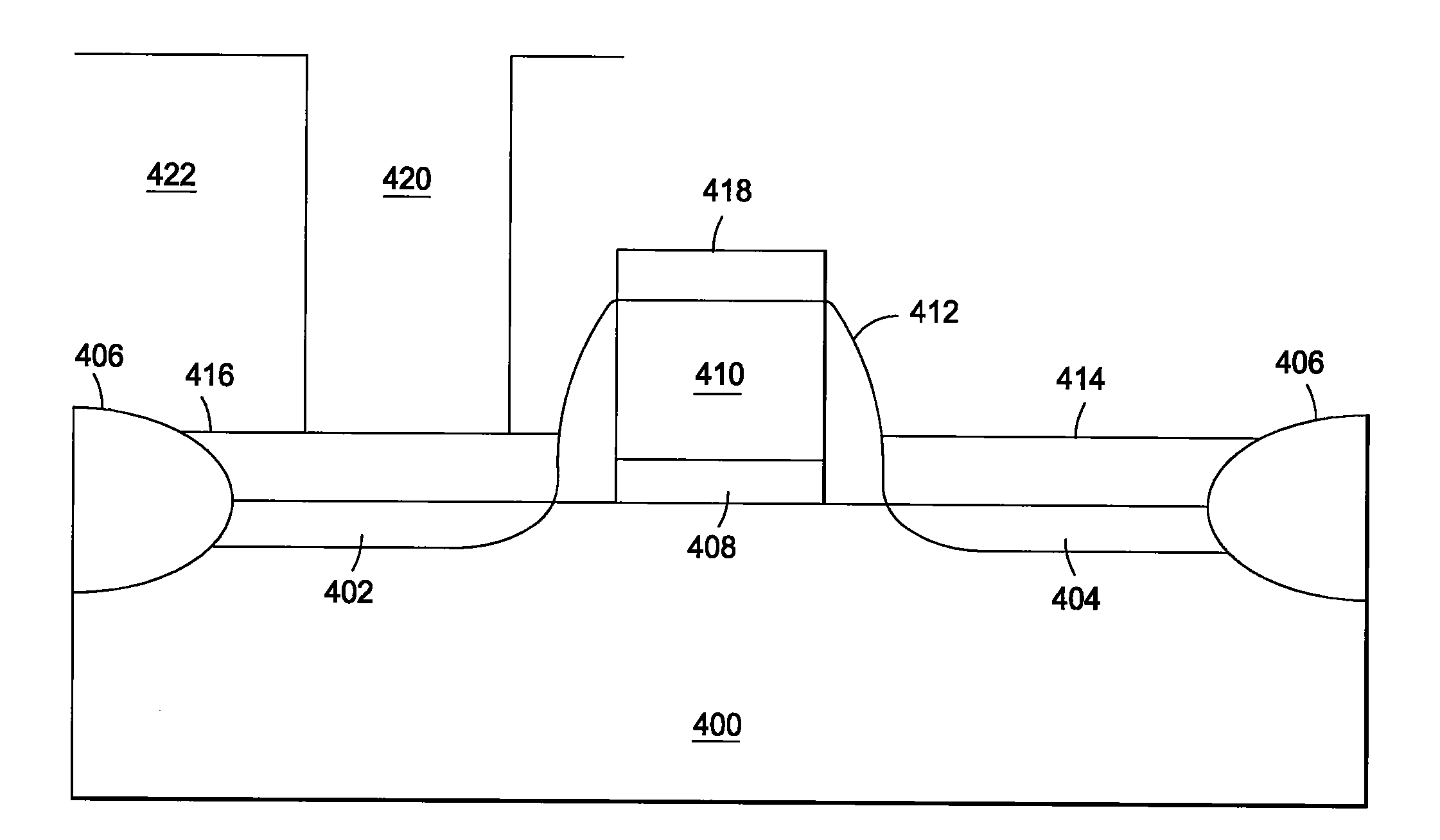
- Description
- Claims
- Application Information
AI Technical Summary
Benefits of technology
Problems solved by technology
Method used
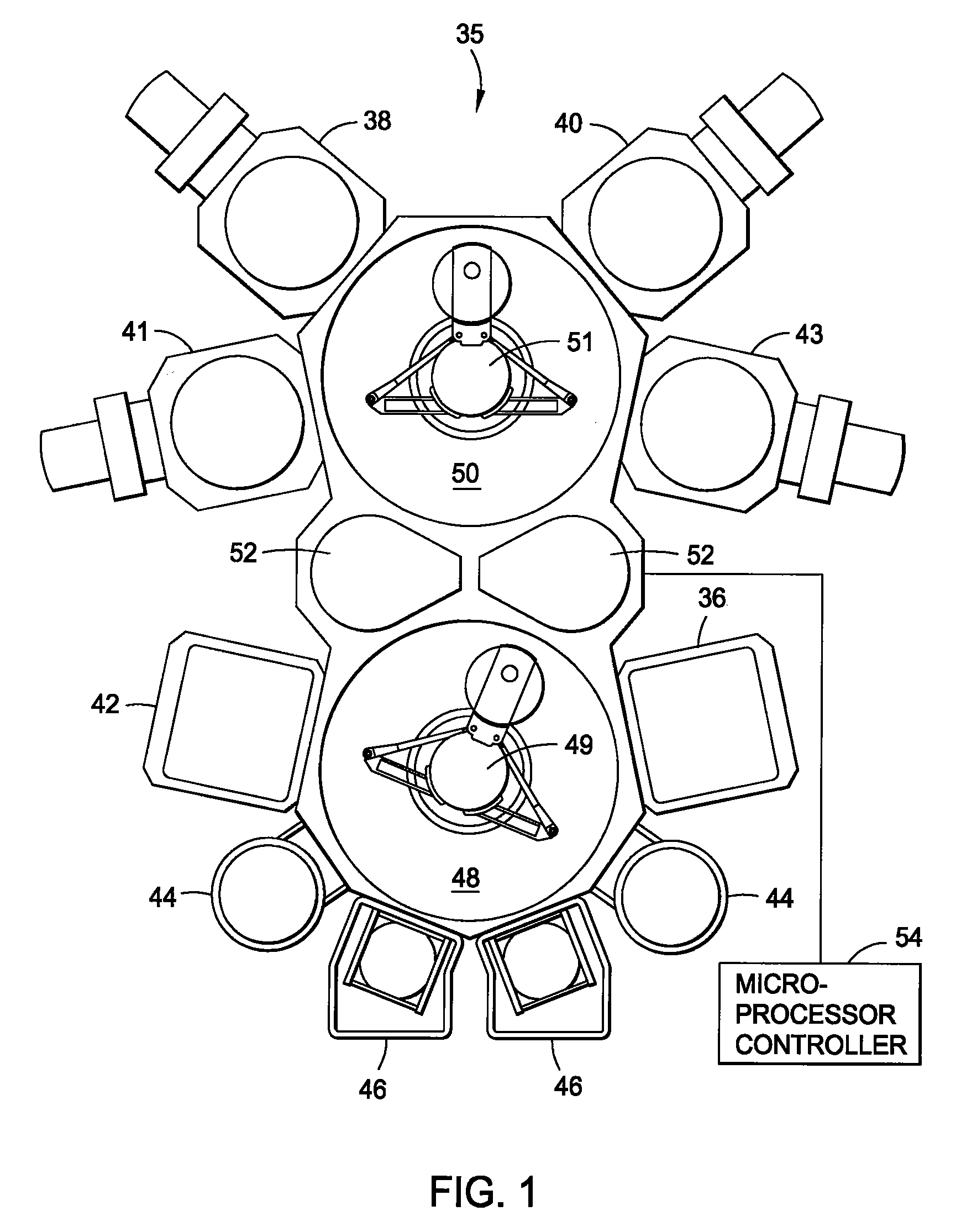
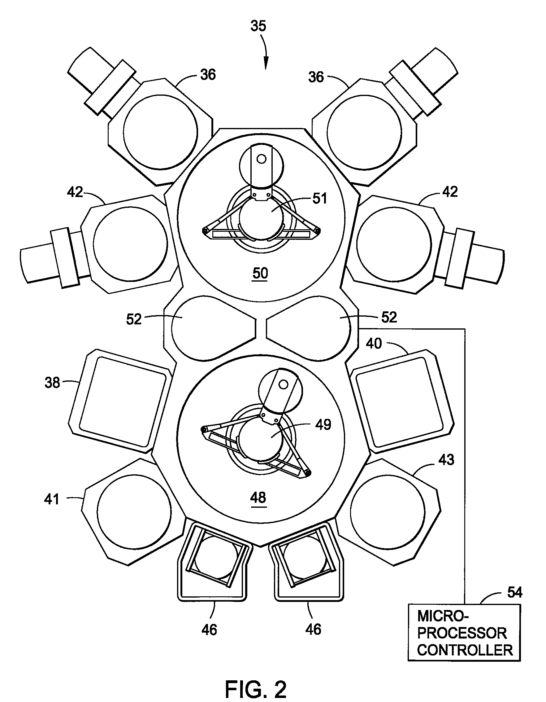
Image

Examples
example 1
[0326]A substrate is treated with at least one preclean process to expose a silicon-containing surface, a cobalt silicide material is deposited over the silicon-containing surface, a metallic cobalt material is deposited over the cobalt silicide material, an optional treatment process may be used to remove cobalt oxides or other surface contaminants, a tungsten material is deposited over the metallic cobalt material, and the tungsten material is exposed to a CMP process. The metallic cobalt material and the cobalt silicide material may be deposited in a first processing chamber, and the optional treatment and the deposition of the tungsten material may be performed in a second processing chamber.
example 2
[0327]A substrate is treated with at least one preclean process to expose a silicon-containing surface, a cobalt silicide material is deposited over the silicon-containing surface, an optional treatment process may be used to remove cobalt oxides or other surface contaminants, a tungsten material (e.g., metallic tungsten) is deposited over the cobalt silicide material, and the tungsten material is exposed to a CMP process. The cobalt silicide material may be deposited in a first processing chamber and the optional treatment and the deposition of the tungsten material may be performed in a second processing chamber.
example 3
[0328]A substrate is treated with at least one preclean process to expose a silicon-containing surface, a cobalt silicide material is deposited over the silicon-containing surface, a metallic cobalt material is deposited over the cobalt silicide material, the substrate is exposed to an annealing process, an optional treatment process may be used to remove cobalt oxides or other surface contaminants, a tungsten material is deposited over the metallic cobalt material, and the tungsten material is exposed to a CMP process. The deposition of the metallic cobalt material and the cobalt silicide material and the annealing process may be performed in a first processing chamber, and the optional treatment and the deposition of the tungsten material may be performed in a second processing chamber.
PUM
| Property | Measurement | Unit |
|---|---|---|
| Concentration | aaaaa | aaaaa |
| Ratio | aaaaa | aaaaa |
| Metallic bond | aaaaa | aaaaa |
Abstract
Description
Claims
Application Information