Light emitting diode devices and manufacturing method thereof

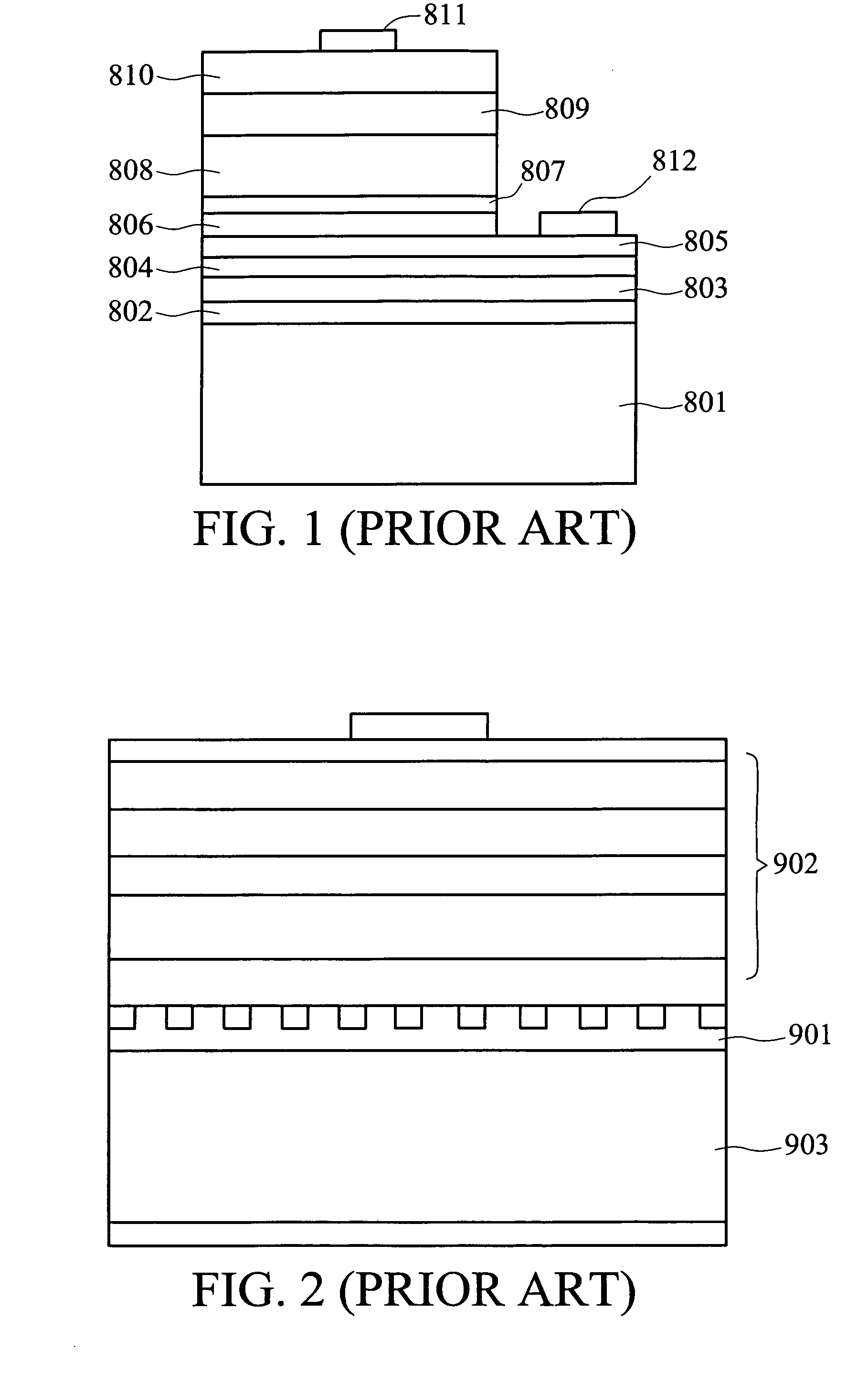
a technology of light-emitting diodes and manufacturing methods, which is applied in the direction of semiconductor/solid-state device manufacturing, semiconductor devices, electrical devices, etc., can solve the problems of not being able to effectively dissipate heat generated by led devices to metal reflective substrates b>801/b>, and the efficiency of led devices is dramatically reduced, so as to reduce the probability of metal particles adhering to the sidewalls of stacked epitaxial structures and reduce residual stress

Active Publication Date: 2009-01-15
DELTA ELECTRONICS INC
View PDF18 Cites 38 Cited by
  • Summary
  • Abstract
  • Description
  • Claims
  • Application Information

AI Technical Summary

Benefits of technology

[0014]Therein, the temporary substrate is a curable polymer material. Because the finished LED device can be obtained by removing the temporary substrate after removing the epitaxial substrate by etching or laser ablation, dicing is not required and the probability of the metal particle adhering to the sidewalls of the stacked epitaxial structure can be reduced. In addition, the heat-conductive plate of the invention has low residual stress and heat corrosion resistance which can prevent the separation between the stacked epitaxial structure and the heat-conductive plate or the damage of the stacked epitaxial structure. The advantageous features of the invention include that product yield can be improved and costs can be reduced.
[0015]As mentioned above, the method for manufacturing a light emitting diode device according to the invention is featured by forming a temporary substrate on a light emitting diode device, and forming at least a heat-conductive plate on the light emitting diode device. Compared with prior art methods, the invention takes advantage of the characteristics of curable polymer material such as its removability, expandability, and ductility to separate the devices naturally to form a plurality of LED devices after easily removing the temporary substrate. Thus, the problem of leakage current generated from the dicing process can be prevented and thus reduce the costs of the dicing process and improve product yield.

Problems solved by technology

However, there are some problems with such LED devices which need to be solved.
However, since the transparent bonding layer 803 is made of plastic materials, the heat generated from the LED device can not transfer to the metal reflective substrate 801 and dissipate effectively.
As a result, the efficiency of the LED device dramatically decreases when the heat inside the LED device continuously accumulates.
However, the metal particle produced in the dicing process can adhere to the sidewalls of the stacked structure and thus increase the leakage current of the stacked structure.
Thus, while an additional dicing process is needed for the method described, the probability of metal particles adhering to the sidewalls of the stacked structure is high.

Method used


Image

  • Light emitting diode devices and manufacturing method thereof
  • Light emitting diode devices and manufacturing method thereof
  • Light emitting diode devices and manufacturing method thereof

Examples


Embodiment Construction

[0022]The following description is of the best-contemplated mode of carrying out the invention. This description is made for the purpose of illustrating the general principles of the invention and should not be taken in a limiting sense. The scope of the invention is best determined by reference to the appended claims.

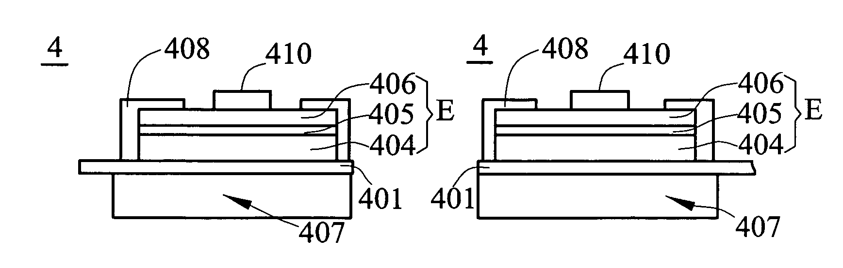
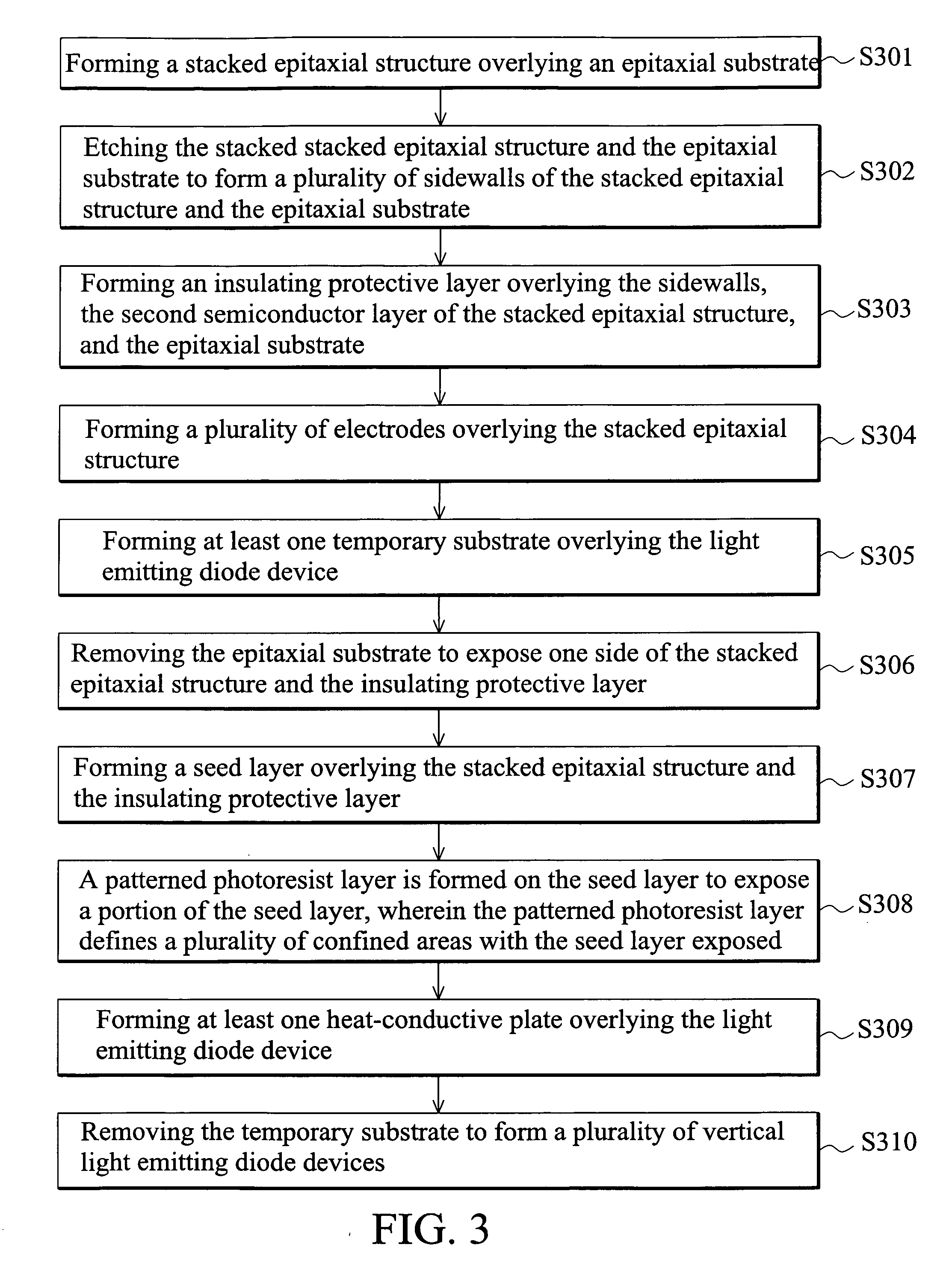
[0023]FIG. 3 is a flow chart showing the manufacturing steps of the LED device according to a preferred embodiment of the invention, wherein the flow chart includes step S301 to step S310. Hereinafter, please also refer to FIG. 4A to FIG. 4H.

[0024]As shown in FIG. 4A, a stacked epitaxial structure on an epitaxial substrate 403 is formed, wherein the stacked epitaxial structure E sequentially includes a first semiconductor layer 404, a light emitting layer 405, and a second semiconductor layer 406 (step S301). The first semiconductor layer 404 is formed on the epitaxial substrate 403, then the light emitting layer 405 is formed on the first semiconductor layer 404, and ...


PUM


Abstract

A light emitting diode (LED) device includes a stacked epitaxial structure, a heat-conductive plate and a seed layer. The stacked epitaxial structure sequentially includes a first semiconductor layer (N—GaN), a light emitting layer, and a second semiconductor layer (P—GaN). The heat-conductive plate is disposed on the first semiconductor layer, and the seed layer is disposed between the first semiconductor layer and the heat-conductive plate. Also, the present invention discloses a manufacturing method thereof including the steps of: forming at least one temporary substrate, which is made by a curable polymer material, on an LED device, and forming at least a heat-conductive plate on the LED device.

Description

BACKGROUND OF THE INVENTION[0001]1. Field of the Invention[0002]The invention relates to a light emitting diode device and a manufacturing method thereof.[0003]2. Description of the Related Art[0004]A light emitting diode (LED) device is a semiconductor luminescent device, providing many advantageous features such as low power consumption, long lifetime, short response time, and so on. The sizes of LED devices are so small that they are easily manufactured to very small devices. Thus, with the continuous improvement of the technology recently, applications of LED devices have been applied in indicator lights of computers or home appliances, back light units of liquid crystal display device, traffic signals, or indicator lights of cars.[0005]According to the prior art, in order to improve luminescence efficiency of LED devices, metal reflective substrates are disposed on LED devices reflecting light to improve luminescence efficiency. However, there are some problems with such LED de...

Claims


Application Information

Patent Timeline
Patent Type & Authority Applications(United States)
IPC IPC(8): H01L33/00H01L33/44H01L33/64
CPCH01L33/0079H01L33/641H01L33/60H01L33/44H01L33/0093
Inventor SHIUE, CHING-CHUANCHEN, SHIH-PENGCHEN, CHAO-MINCHEN, HUANG-KUN
Owner DELTA ELECTRONICS INC
Why Eureka
Try Eureka