CMOS image sensor with photo-detector protecting layers
a technology of image sensor and protective layer, applied in the field of image sensors, can solve the problems of high power consumption of ccds, difficulty in integrating peripheral circuits into one-chip systems, and random nois
- Summary
- Abstract
- Description
- Claims
- Application Information
AI Technical Summary
Benefits of technology
Problems solved by technology
Method used
Image

Examples
Embodiment Construction
[0034]The present invention is now described more fully with reference to the accompanying drawings, in which exemplary embodiments of the invention are shown. However, such embodiments are not intended to limit the scope of the present invention that may be implemented in other forms. The embodiments as described herein are for thoroughly and completely disclosing the present invention to those of ordinary skill in the art. The dimensions of any layers and regions in the drawings may be exaggerated for clarity of illustration.
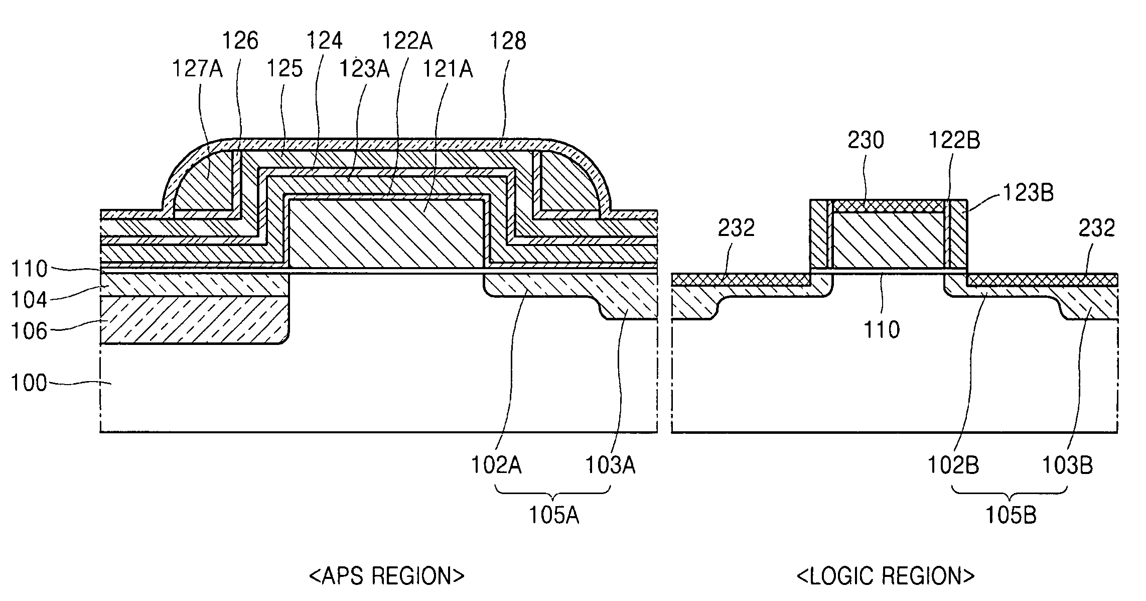
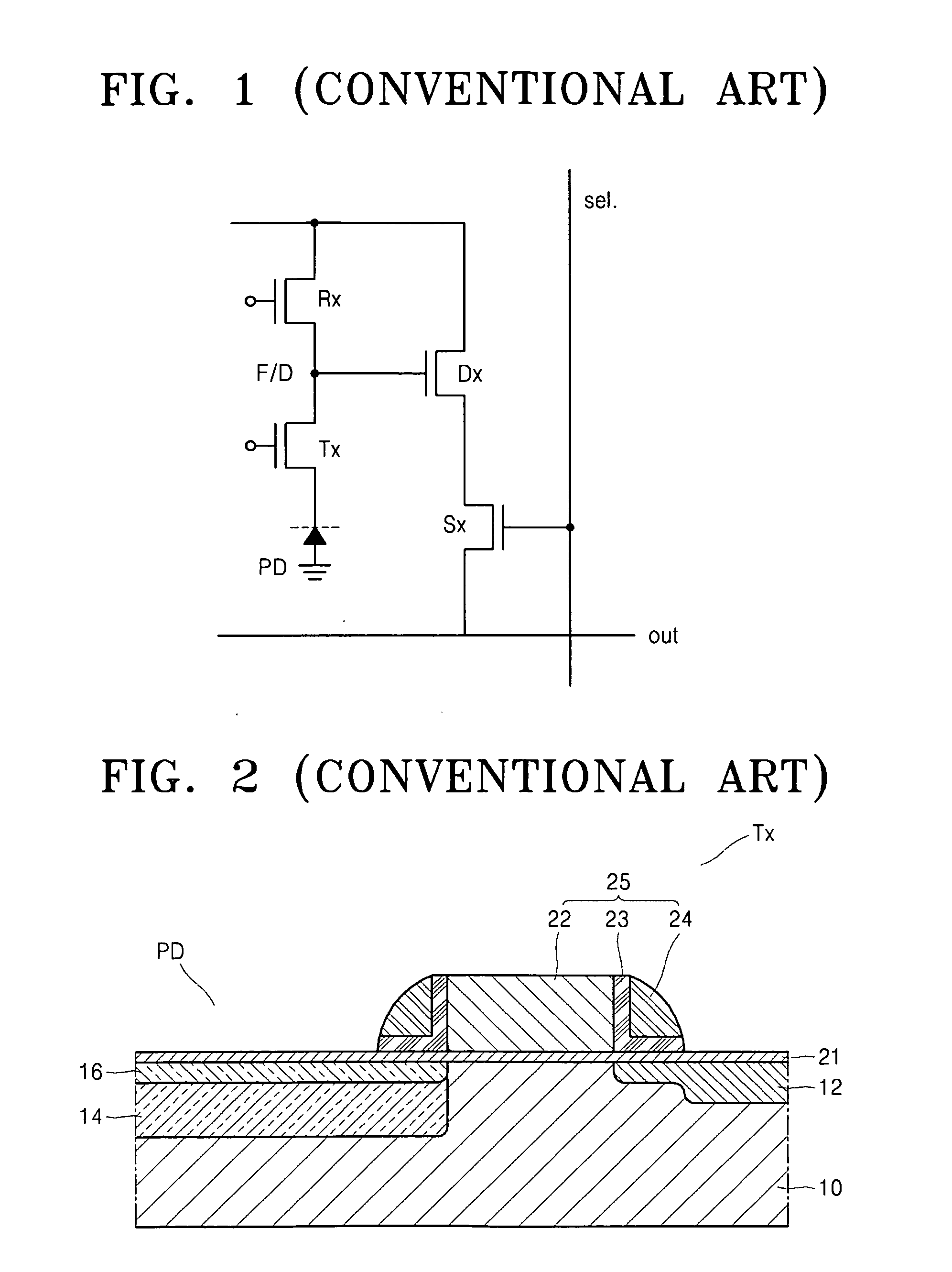
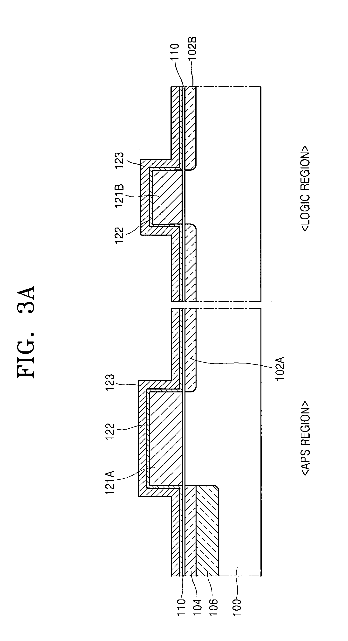
[0035]FIGS. 3A, 3B, 3C, 3D, 3E, 3F, 3G, and 3H show cross-sectional views of an APS (active pixel sensor) region and a logic region during fabrication of a CMOS image sensor according to an embodiment of the present invention. In particular, such FIGS. 3A, 3B, 3C, 3D, 3E, 3F, 3G, and 3H illustrate a photo-diode and a transfer transistor of an example unit pixel formed in the APS region with multiple photodiode protecting layers and an example field effect tran...
PUM
 Abstract
Description
Claims
Application Information