Reactive flow deposition and synthesis of inorganic foils

a technology of inorganic foils and reactive fluxes, which is applied in the direction of chemically reactive gases, solid-state diffusion coatings, record information storage, etc., can solve the problems that renewable energy sources do not produce green house gases, and achieve the effects of facilitating reaction, enhancing particulate release layers, and reducing the formation of vapors

Inactive Publication Date: 2009-01-15
NANOGRAM
View PDF66 Cites 25 Cited by
  • Summary
  • Abstract
  • Description
  • Claims
  • Application Information

AI Technical Summary

Problems solved by technology

Furthermore, renewable energy sources do not produce green house gases that can contribute to global warming.

Method used


Image

  • Reactive flow deposition and synthesis of inorganic foils
  • Reactive flow deposition and synthesis of inorganic foils
  • Reactive flow deposition and synthesis of inorganic foils

Examples


example 1

Scanning Sub-Atmospheric Pressure CVD onto a Release Layer

[0132]This example demonstrates the ability to deposit a high quality silicon foil layer using scanning sub-atmospheric pressure CVD onto a release layer formed using light reactive deposition.

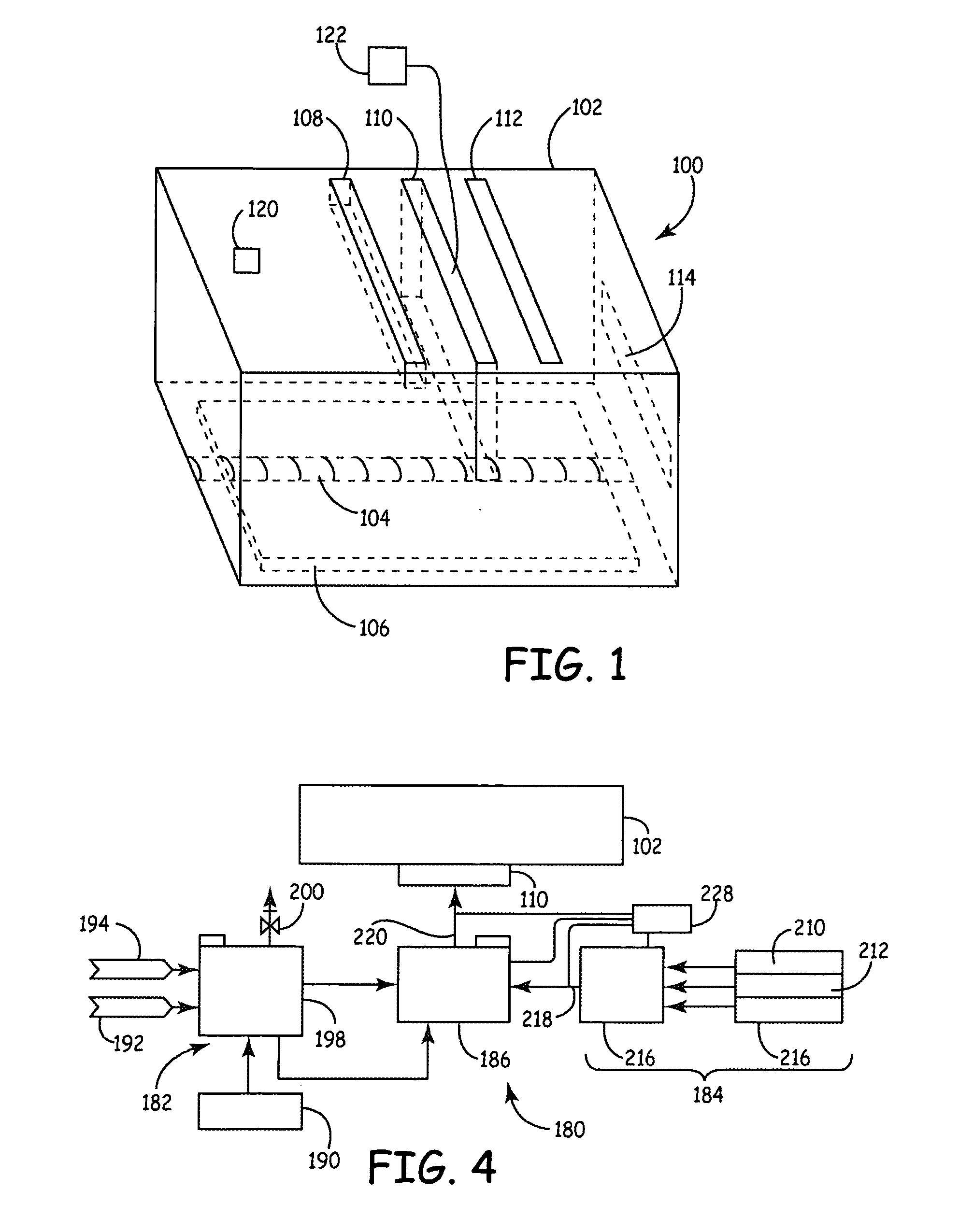
[0133]The depositions were performed in a reactor essentially as described in published U.S. patent application 2007 / 0212510, filed Mar. 13, 2007 to Hieslmair et al., entitled “Thin Silicon or Germanium Sheets and Photovoltaics Formed From Thin Sheets,” incorporated herein by references. The CVD deposition was performed with the laser turned off using the same reactant supply system with appropriately selected reactants delivered for the particular deposition process.

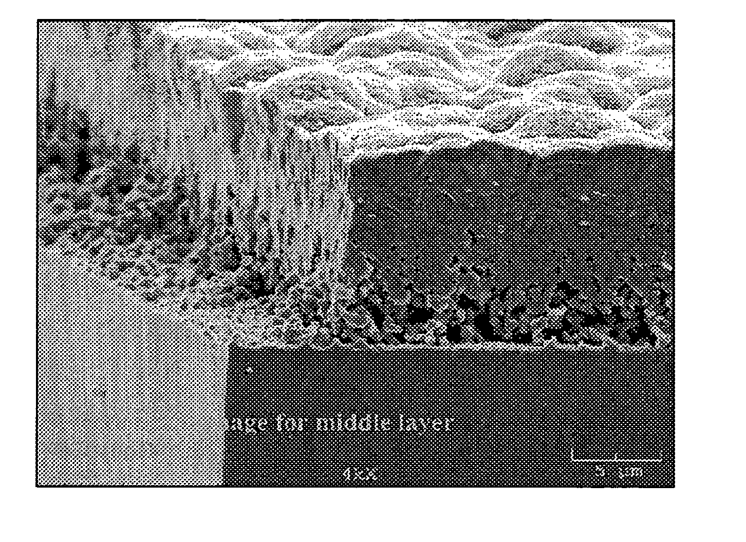
[0134]A stack of deposited layers is shown in the FIG. 8. Starting from the bottom of the micrograph, the layers can be identified as follows: substrate, micron porous silicon nitride layer formed with light reactive deposition and a dense CVD silicon film. Two other repres...

example 2

Separation of Silicon Foil at the Release Layer

[0136]This example demonstrates the ability to separate a silicon foil through the fracture of a porous particulate release layer.

[0137]A series of depositions was performed to form a structure essentially as described above with respect to FIG. 9. In general, samples have been formed generally at about 600 Torr or lower pressures with layers generally within the ranges of 10 to 40 microns of porous particulate silicon nitride formed by light reactive deposition, 5 to 10 microns of SSAP-CVD silicon nitride, about 35 microns of SSAP-CVD silicon and a thin silicon nitride capping layer. After deposition, the silicon was subjected to a zone melt recrystallization process. In the ZMR process, the structure was scanned past a radiant heater to melt the silicon, which subsequently recrystallizes as the material cools. A photograph of the resulting structure is shown in FIG. 11.

[0138]To perform the separation, a crosslinking ethylenevinylaceta...


PUM

PropertyMeasurementUnit
pressureaaaaaaaaaa
pressureaaaaaaaaaa
pressureaaaaaaaaaa

Abstract

Sub-atmospheric pressure chemical vapor deposition is described with a directed reactant flow and a substrate that moves relative to the flow. Thus, using this CVD configuration a relatively high deposition rate can be achieved while obtaining desired levels of coating uniformity. Deposition approaches are described to place one or more inorganic layers onto a release layer, such as a porous, particulate release layer. In some embodiments, the release layer is formed from a dispersion of submicron particles that are coated onto a substrate. The processes described can be effective for the formation of silicon films that can be separated with the use of a release layer into a silicon foil. The silicon foils can be used for the formation of a range of semiconductor based devices, such as display circuits or solar cells.

Description

CROSS REFERENCE TO RELATED APPLICATIONS[0001]This application claims priority to copending U.S. provisional patent application Ser. No. 60 / 934,793 filed on Jun. 15, 2007 to Hieshnair et al., entitled “Sub-Atmospheric Pressure CVD,” and to copending U.S. provisional patent application Ser. No. 61 / 062,398 filed on Jan. 25, 2008 to Hieslmair et al., entitled “Deposition Onto a Release Layer for Synthesizing Inorganic Foils,” both of which are incorporated herein by reference.FIELD OF THE INVENTION[0002]The invention relates to deposition at sub-atmospheric pressures using chemical vapor deposition. Furthermore, the invention relates to reactive deposition approaches, such as chemical vapor deposition and light reactive deposition, onto a release layer for the formation of an inorganic foil that can be separated from the release layer. Corresponding methods and applications of the inorganic foils are described, in particular for foils formed from elemental silicon.BACKGROUND OF THE INVE...

Claims


Application Information

Patent Timeline
Patent Type & Authority Applications(United States)
IPC IPC(8): B32B5/00C23C16/00C23C16/513B05D1/00B01J19/12B05D1/36C23C16/44
CPCC23C16/01Y10T428/264C23C16/545C30B13/00C30B25/02C30B25/18C30B29/06H01L21/02488H01L21/02513H01L21/02532H01L31/1804H01L31/1872H01L31/202Y02E10/547Y10T428/263Y10T428/265Y10T428/26C23C16/24Y02P70/50C23C16/50C23C16/455C23C16/44H01L21/0262
Inventor HIESLMAIR, HENRYMOSSO, RONALD J.SOLAYAPPAN, NARAYANCHIRUVOLU, SHIVKUMARMORRIS, JULIO E.
Owner NANOGRAM
Why Eureka
Try Eureka