

Semiconductor device
a technology of semiconductor devices and semiconductors, applied in the direction of semiconductor devices, electrical equipment, transistors, etc., can solve the problems of inability to arrange wirings and contacts in an unoccupied area even in an area over the standard cell, and achieve the effect of high integration of semiconductor devices
- Summary
- Abstract
- Description
- Claims
- Application Information
AI Technical Summary
Benefits of technology
Problems solved by technology
Method used
Image

Examples
embodiment 1
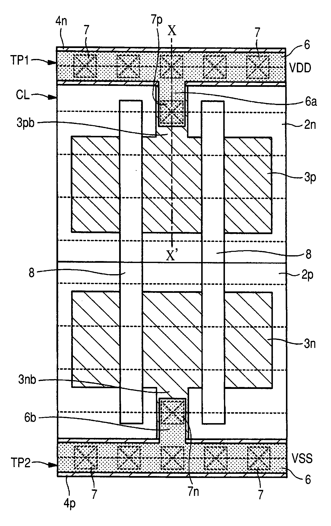
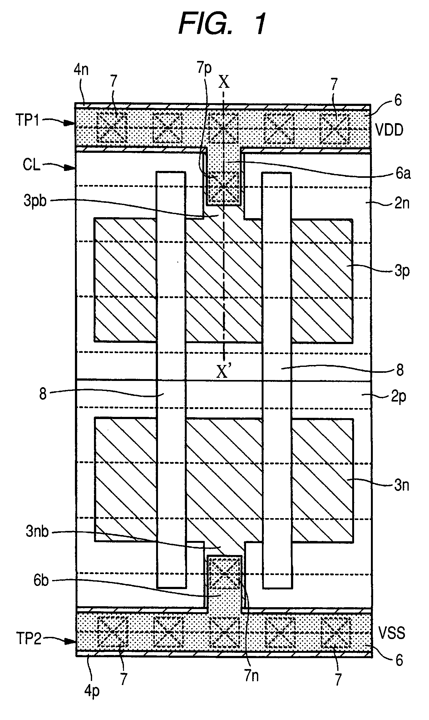
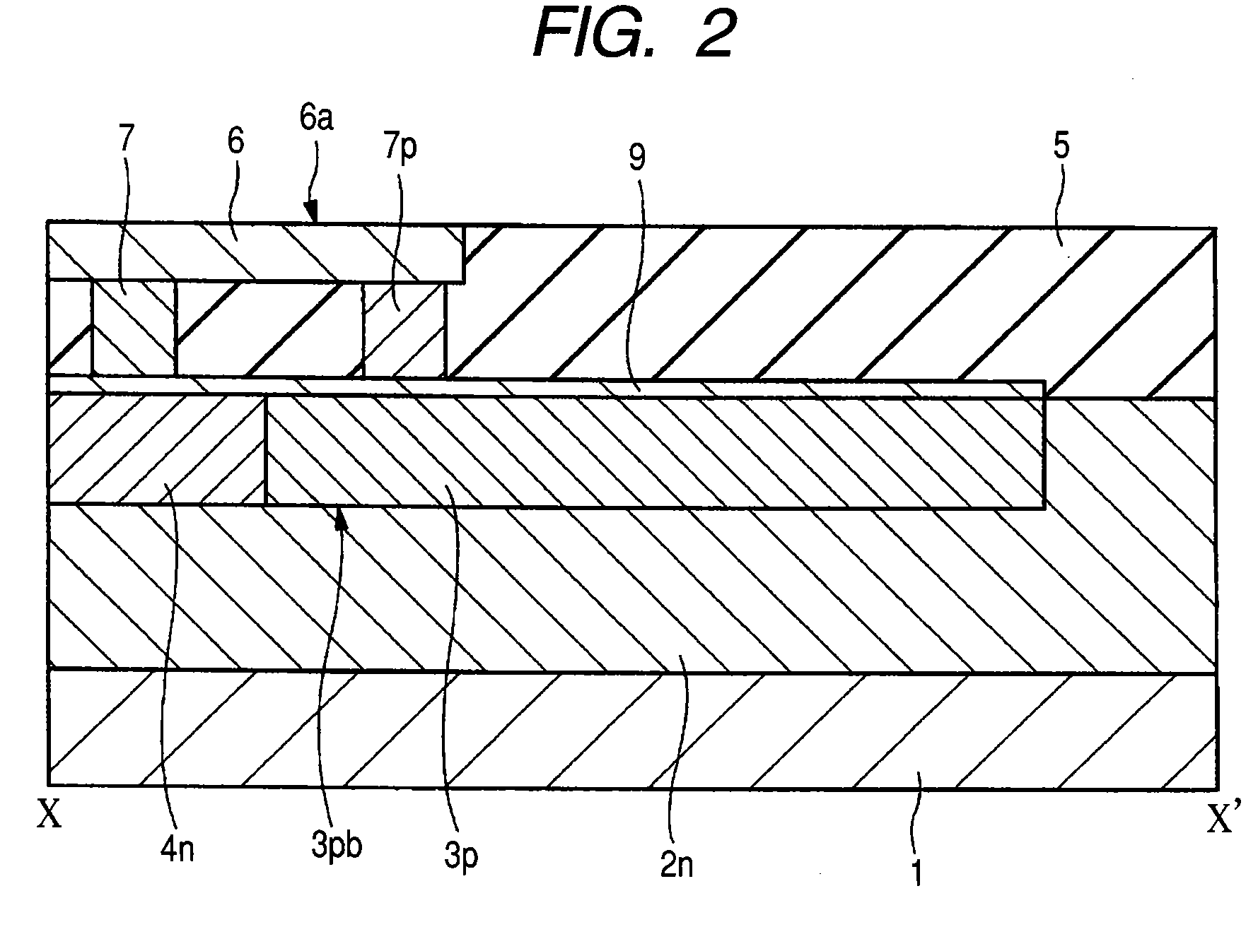
[0032]FIG. 1 is a plan view (layout pattern) of a principal part schematically showing an LSI (semiconductor device) in Embodiment 1 of the present invention, and FIG. 2 is a cross sectional view along an X-X′ line of FIG. 1. For example, on a major side (surface for forming elements) of a semiconductor substrate (hereinafter, referred to as a substrate) 1 composed of an n−-type single crystal silicon, a standard cell (logic circuit cell) CL and taps TP1, TP2 are laid out. The standard cell CL is configured using an MIS (Metal Insulator Semiconductor) transistor as a semiconductor element. Note that the MIS transistor, and a contact and a wiring layer thereabove can be formed using a well-known manufacturing method.
[0033]In the major side of the substrate 1 in which the standard cell CL and the taps TP1, TP2 are formed, an n-type well 2n and a p-type well 2p comprising n-type and p-type impurities, respectively, which are introduced using a photolithography technique and an ion impl...
embodiment 2
[0054]FIG. 6 is a plan view (layout pattern) of a principal part schematically showing an LSI (semiconductor device) in Embodiment 2 of the present invention. The layout pattern of the LSI in this Embodiment 2 is, as shown in FIG. 6, a combination of the layout pattern of the present invention described in the above Embodiment 1 and the layout pattern studied in the Embodiment 1. Furthermore, even if the layout pattern of the present invention and the studied layout pattern are arranged vertically or horizontally, the boundary condition thereof will not be added in particular.
[0055]By applying the present invention to the standard cell this way, the layout pattern can be given a degree of freedom.
embodiment 3
[0056]FIG. 7 is a plan view (layout pattern) of a principal part schematically showing an LSI (semiconductor device) in Embodiment 3 of the present invention, and FIG. 8 is a cross sectional view along a Y-Y′ line of FIG. 7. While the above Embodiment 1 shows the case where the power supply VDD is supplied from the first-layer wiring layer 6, this Embodiment 3 shows the case where the power supply VDD is supplied from the second-layer wiring layer 10. Even in the case where the second-layer wiring layer 10 is used for the power supply VDD, the same effect as that of the above Embodiment 1 can be obtained.
PUM
 Abstract
Description
Claims
Application Information