ESD protection for bipolar-CMOS-DMOS integrated circuit devices

a technology of integrated circuit devices and cmos, which is applied in the direction of semiconductor devices, semiconductor/solid-state device details, electrical apparatus, etc., can solve the problems of reducing the esd energy distribution efficiency of cmos, so as to achieve the effect of high doping concentration

Inactive Publication Date: 2009-02-05
ADVANCED ANALOGIC TECHNOLOGIES INCORPORATED +1
View PDF21 Cites 48 Cited by
  • Summary
  • Abstract
  • Description
  • Claims
  • Application Information

AI Technical Summary

Benefits of technology

[0014]The doped regions that constitute the isolation structure and the doped regions that constitute the ESD protection device are preferably formed by single or multiple implants with essentially no thermal processes that would result in the diffusion of the dopants. These doped regions therefore remain in an essentially “as-implanted” configuration. The process flow is modular in the sense that, with a few exceptions, the implants may be performed in virtually any order, and it is possible to eliminate one or more process steps in the fabrication of a given IC, depending on which set of devices are required.

Problems solved by technology

ESD devices with higher trigger voltages generally rely on a lateral breakdown mechanism that is prone to current crowding, making it difficult to design large structures that effectively distribute the ESD energy.
Fabrication of conventional CMOS in P-type substrate material does not facilitate complete isolation of its devices since every P-type well forming the body (back-gate) of NMOS transistors is shorted to the substrate potential, typically the most negative on-chip potential.
High temperature processing causes a redistribution of dopant atoms in the substrate and epitaxial layers, causing unwanted tradeoffs and compromises in the manufacturing of dissimilar devices fabricated using one common process.
Moreover, the high-temperature diffusions and epitaxy employed in epi-JI processes are generally incompatible with the large wafer diameters and advanced low-temperature processing equipment common in submicron CMOS fabs.

Method used


Image

  • ESD protection for bipolar-CMOS-DMOS integrated circuit devices
  • ESD protection for bipolar-CMOS-DMOS integrated circuit devices
  • ESD protection for bipolar-CMOS-DMOS integrated circuit devices

Examples


Embodiment Construction

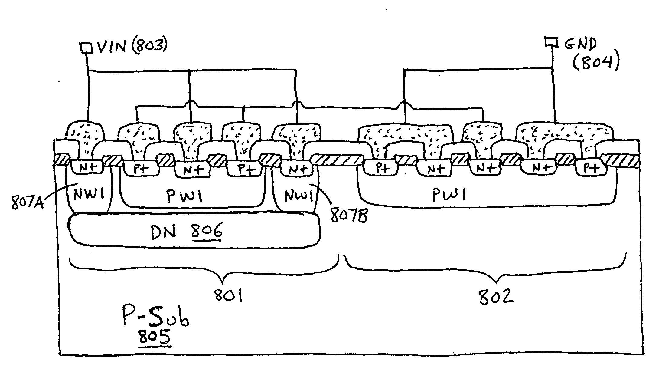
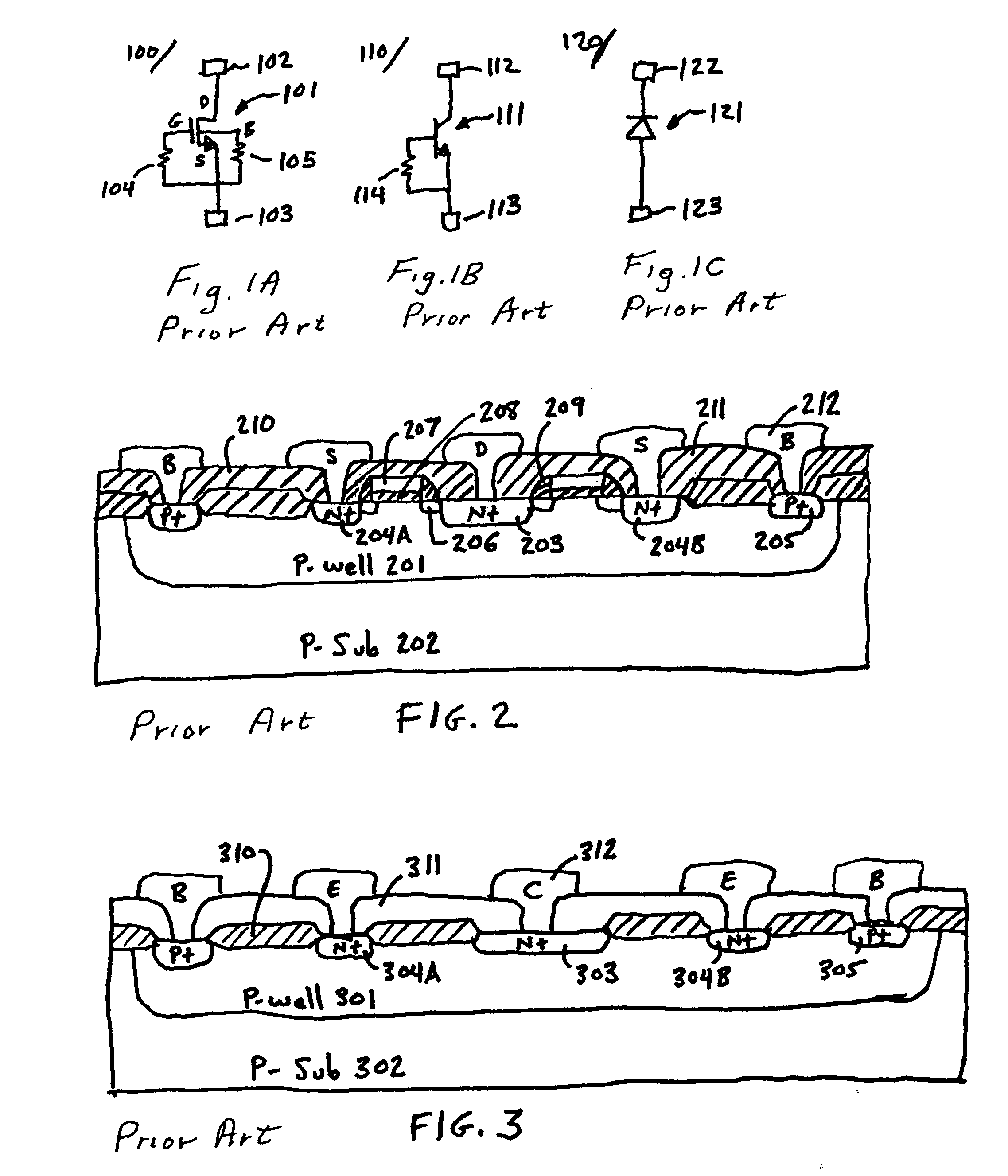
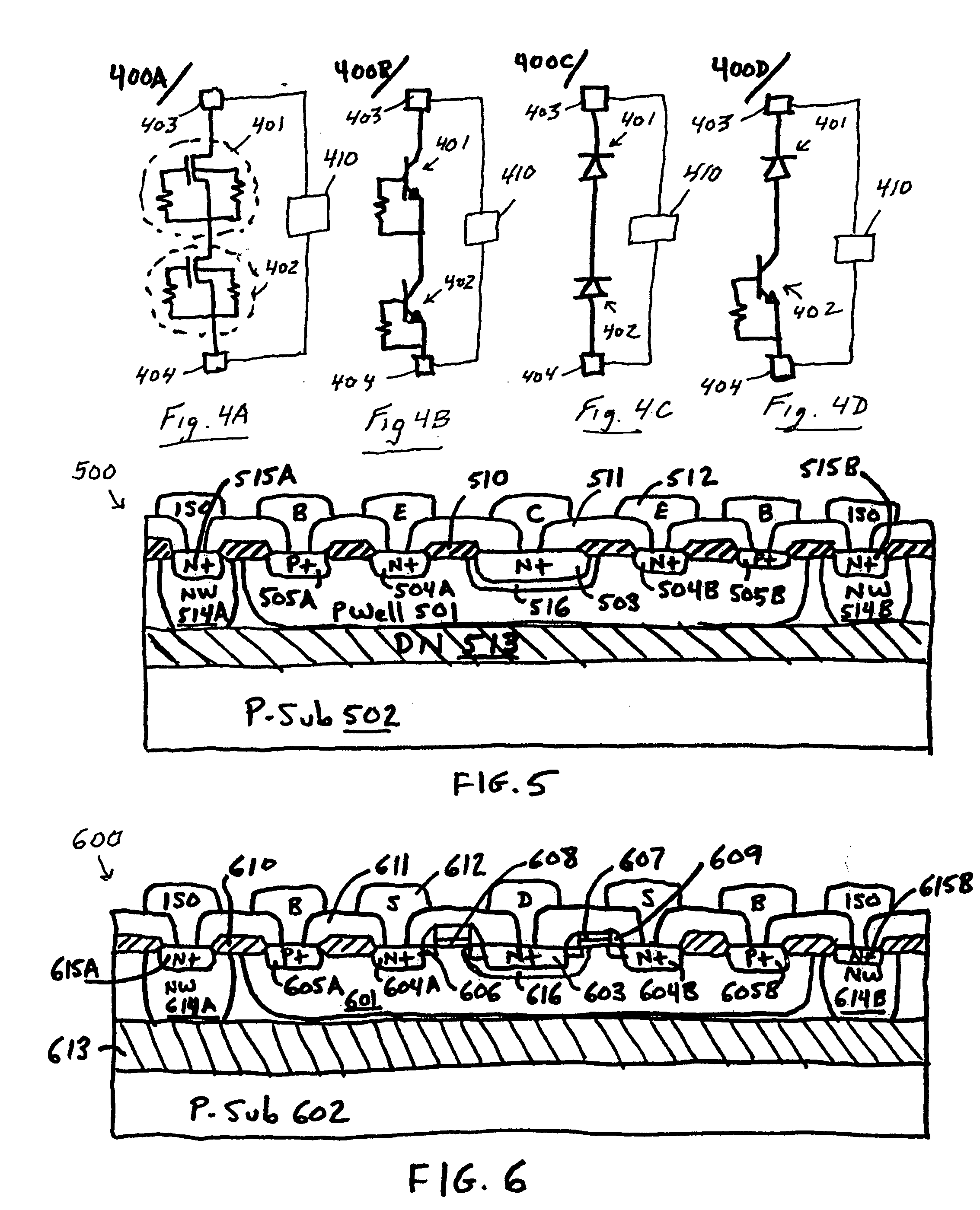
[0024]An all low-temperature fabrication method using as-implanted junction isolation structures employs high-energy and chain implants with dopant implanted through contoured oxides to achieve fully-isolated bipolar, CMOS and DMOS devices without the need for isolation diffusions, epitaxy or high temperature processes. The low-temperature wafer fabrication methods and isolated device structures were previously described in pending U.S. Application No. 11 / 298,075 and in U.S. Pat. Nos. 6,855,985, 6,900,091 and 6,943,426 to R. K. Williams et al., each of which is incorporated herein by reference.

[0025]The inventive matter in this application is related to these patents and applications but concentrates on the design and integration of isolated and stackable ESD protection structures.

[0026]The low-temperature fabrication of the high-voltage devices described in this application are compatible with the modular low-temperature fabrication methods described in the aforementioned applicati...


PUM


Abstract

An Electro-Static Discharge (ESD) protection device is formed in an isolated region of a semiconductor substrate. The ESD protection device may be in the form of a MOS or bipolar transistor or a diode. The isolation structure may include a deep implanted floor layer and one or more implanted wells that laterally surround the isolated region. The isolation structure and ESD protection devices are fabricated using a modular process that includes virtually no thermal processing. Since the ESD device is isolated, two or more ESD devices may be electrically “stacked” on one another such that the trigger voltages of the devices are added together to achieve a higher effective trigger voltage.

Description

CROSS-REFERENCE TO RELATED APPLICATION[0001]This application is a divisional of application Ser. No. 11 / 499,381, filed Aug. 4, 2006, which is incorporated herein by reference in its entirety.FIELD OF THE INVENTION[0002]This invention relates to semiconductor chip fabrication and in particular to methods of fabricating and electrically isolating bipolar, CMOS and DMOS transistors and passive components in a semiconductor chip monolithically at high densities without the need for high temperature fabrication processing steps, and to provide ESD protection for such devices.BACKGROUND OF THE INVENTION[0003]In the fabrication of integrated circuit (IC) chips, it is frequently necessary to electrically isolate devices that are formed on the surface of the chip, especially when these components operate at different voltages. Such complete electrical isolation is necessary to integrate certain types of transistors including bipolar junction transistors and various metal-oxide-semiconductor ...

Claims


Application Information

Patent Timeline
Patent Type & Authority Applications(United States)
IPC IPC(8): H02H9/04H01L27/06
CPCH01L27/0251H01L29/0626H01L29/0692H01L29/866H01L29/735H01L29/7833H01L29/861H01L29/7317
Inventor DISNEY, DONALD RAYCHEN, JUN-WEIWILLIAMS, RICHARD K.RYU, HYUNGSIKCHAN, WAI TIEN
Owner ADVANCED ANALOGIC TECHNOLOGIES INCORPORATED
Why Eureka
Try Eureka