Method of forming dielectric layers on a substrate and apparatus therefor

a technology of dielectric layers and substrates, applied in the field of semiconductor processing, can solve the problems of poor surface roughness, process and/or device performance variability, poor film quality, etc., and achieve the effect of rapid thermal process

Inactive Publication Date: 2009-02-05
APPLIED MATERIALS INC
View PDF35 Cites 300 Cited by
  • Summary
  • Abstract
  • Description
  • Claims
  • Application Information

AI Technical Summary

Problems solved by technology

However, CVD processes typically result in poor roughness of the surface, leading to process and or device performance variability.
In addition, ALD processes typically have deposition initiation and incubation problems, resulting in poor film quality, reduced initial deposition rates, and high process variability.

Method used


Image

  • Method of forming dielectric layers on a substrate and apparatus therefor
  • Method of forming dielectric layers on a substrate and apparatus therefor
  • Method of forming dielectric layers on a substrate and apparatus therefor

Examples


Embodiment Construction

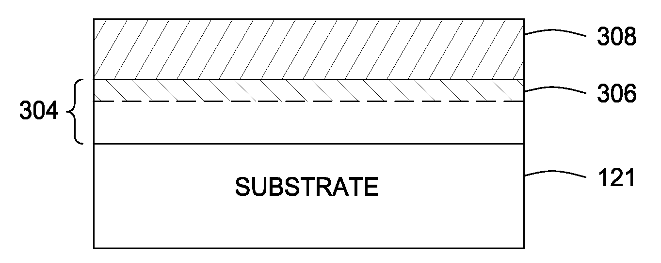
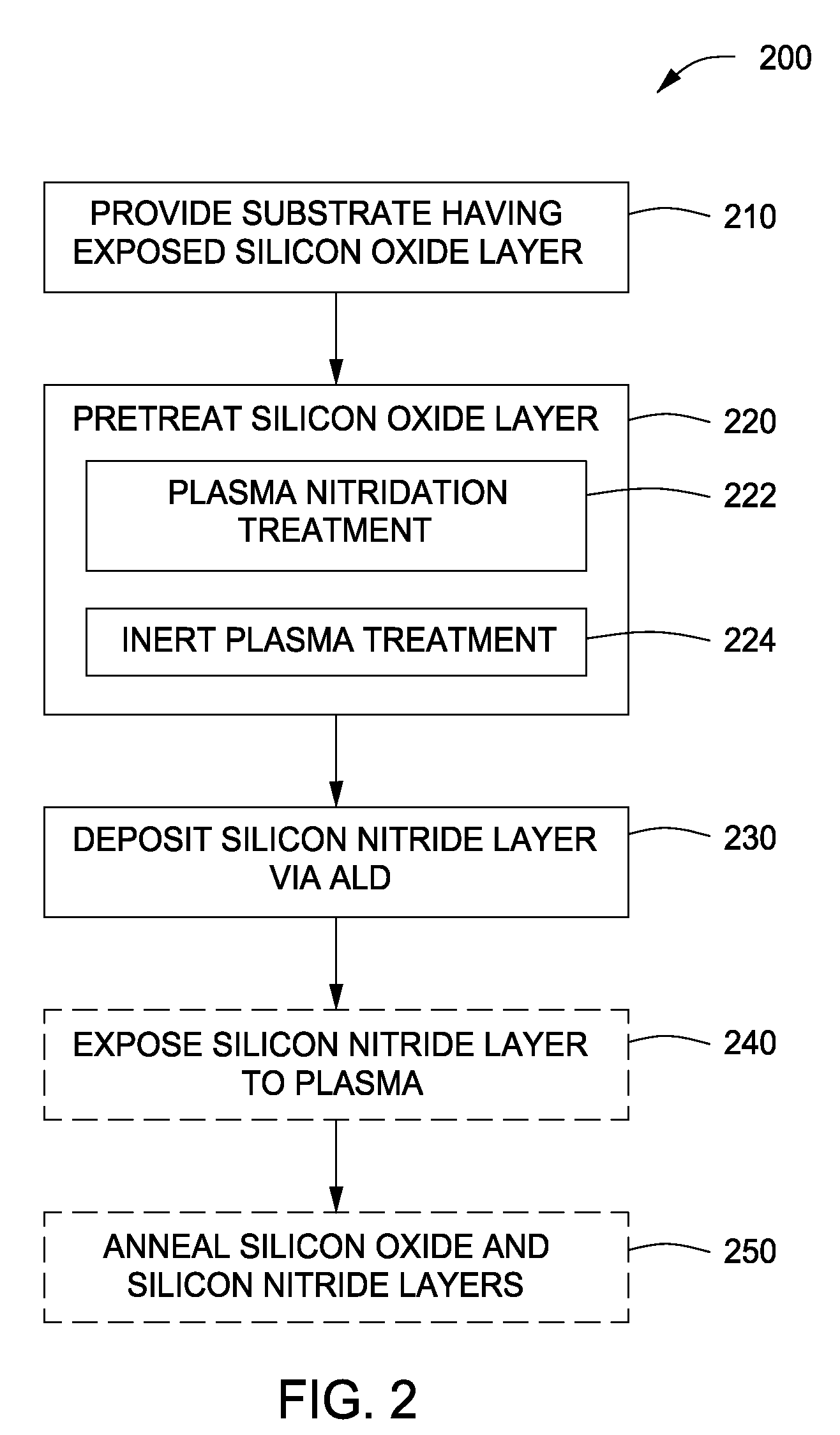
[0018]Embodiments of the present invention generally provide methods for fabricating dielectric materials used in a variety of applications, for example, as a gate dielectric layer used in field effect transistors fabrication. In some embodiments improved methods of forming a silicon nitride film be atomic layer deposition (ALD) is provided. ALD nitride layers formed in accordance with embodiments of the present invention may have improved deposition rates and / or film quality as compared to conventional ALD nitride layers. In some embodiments, the improved ALD nitride layer may form part of a gate dielectric stack, for example, for use in a transistor.

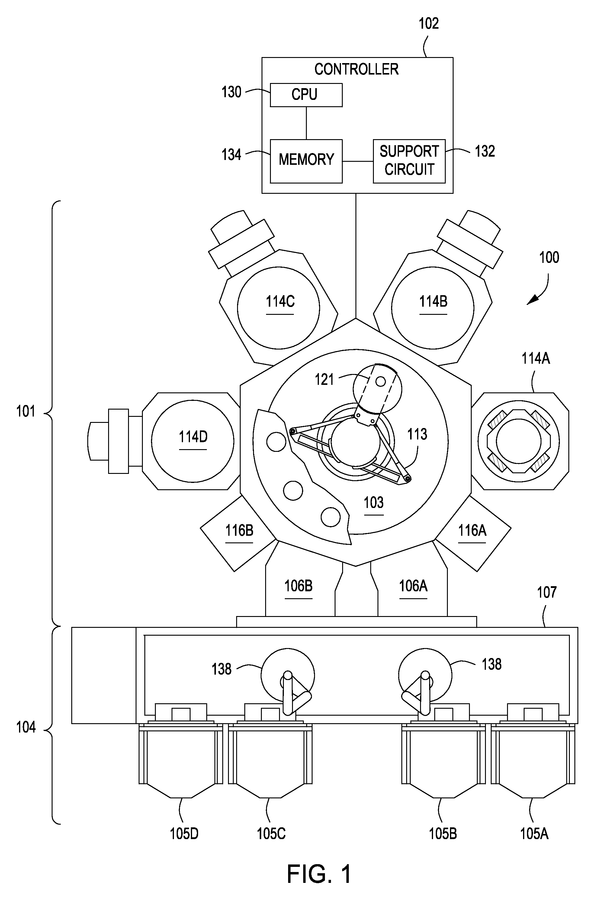
[0019]FIG. 1 is a schematic view of an integrated tool 100 (e.g., a cluster tool) suitable for processing semiconductor substrates according to embodiments of the present invention. Examples of the integrated tool 100 include the CENTURA® and ENDURA® integrated tool, both available from Applied Materials, Inc., of Santa Clara, Calif. I...


PUM

PropertyMeasurementUnit
temperatureaaaaaaaaaa
frequencyaaaaaaaaaa
diameteraaaaaaaaaa

Abstract

Methods of forming dielectric layers on a substrate comprising silicon and oxygen are disclosed herein. In some embodiments, a method of forming a dielectric layer on a substrate includes provide a substrate having an exposed silicon oxide layer; treating an upper surface of the silicon oxide layer with a plasma; and depositing a silicon nitride layer on the treated silicon oxide layer via atomic layer deposition. The silicon nitride layer may be exposed to a plasma nitridation process. The silicon oxide and silicon nitride layers may be subsequently thermally annealed. The dielectric layers may be used as part of a gate structure.

Description

BACKGROUND OF THE INVENTION[0001]1. Field of the Invention[0002]Embodiments of the present invention generally relate to semiconductor processing, and more specifically, to methods for fabricating dielectric materials on a substrate.[0003]2. Description of the Related Art[0004]Integrated circuits may include more than one million micro-electronic field effect transistors (e.g., complementary metal-oxide-semiconductor (CMOS) field effect transistors) that are formed on a substrate (e.g., semiconductor wafer) and cooperate to perform various functions within the circuit. A CMOS transistor comprises a gate structure disposed between source and drain regions that are formed in the substrate. The gate structure generally comprises a gate electrode and a gate dielectric layer. The gate electrode is disposed over the gate dielectric layer to control a flow of charge carriers in a channel region formed between the drain and source regions beneath the gate dielectric layer.[0005]Some exempla...

Claims


Application Information

Patent Timeline
Patent Type & Authority Applications(United States)
IPC IPC(8): H01L21/31C23C16/00H01L21/3205
CPCC23C16/0272C23C16/345C23C16/56H01L29/792H01L21/3144H01L21/3185H01L29/66833H01L21/3141H01L21/02238H01L21/02164H01L21/02255H01L21/022H01L21/0228H01L21/0217H01L21/0234
Inventor OLSEN, CHRISTOPHER S.GOYANI, TEJALSWENBERG, JOHANES
Owner APPLIED MATERIALS INC
Why Eureka
Try Eureka