SiC Crystal Semiconductor Device

a semiconductor device and crystal technology, applied in the direction of crystal growth process, polycrystalline material growth, chemistry apparatus and processes, etc., can solve the problems of insufficient improvement, difficult or impossible to remove native intrinsic defects, and still contain native intrinsic defects, etc., to achieve effective reduction or elimination of carrier trapping centers, excellent device characteristics

Active Publication Date: 2009-02-12
CENTRAL RESEARCH INSTITUTE OF ELECTRIC POWER INDUSTRY
View PDF10 Cites 19 Cited by
  • Summary
  • Abstract
  • Description
  • Claims
  • Application Information

AI Technical Summary

Benefits of technology

[0027]An object of the present invention is to provide a method of effectively reducing or eliminating the carrier trapping centers by high temperature annealing.

Problems solved by technology

Although SiC layers of excellent quality are available at present, they still contain native intrinsic defects which act as carrier traps and degrade materials characteristics.
The high thermal stability of SiC makes it usually difficult or impossible to remove these defects by a thermal treatment (anneal out).
However, in the case of an SiC monocrystal, the improvement is not sufficient due to the above described high thermal stability.

Method used


Image

  • SiC Crystal Semiconductor Device
  • SiC Crystal Semiconductor Device
  • SiC Crystal Semiconductor Device

Examples


Embodiment Construction

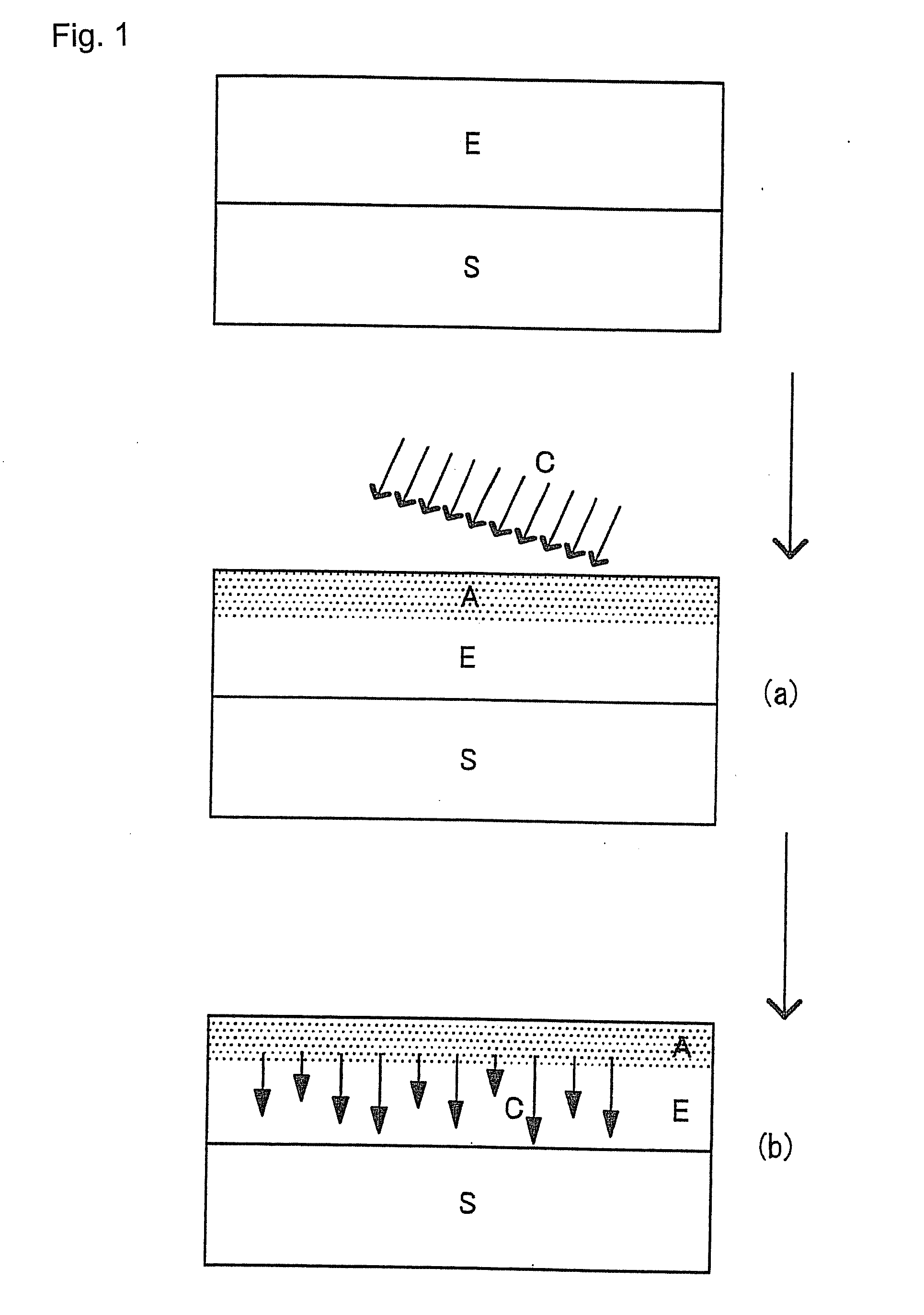
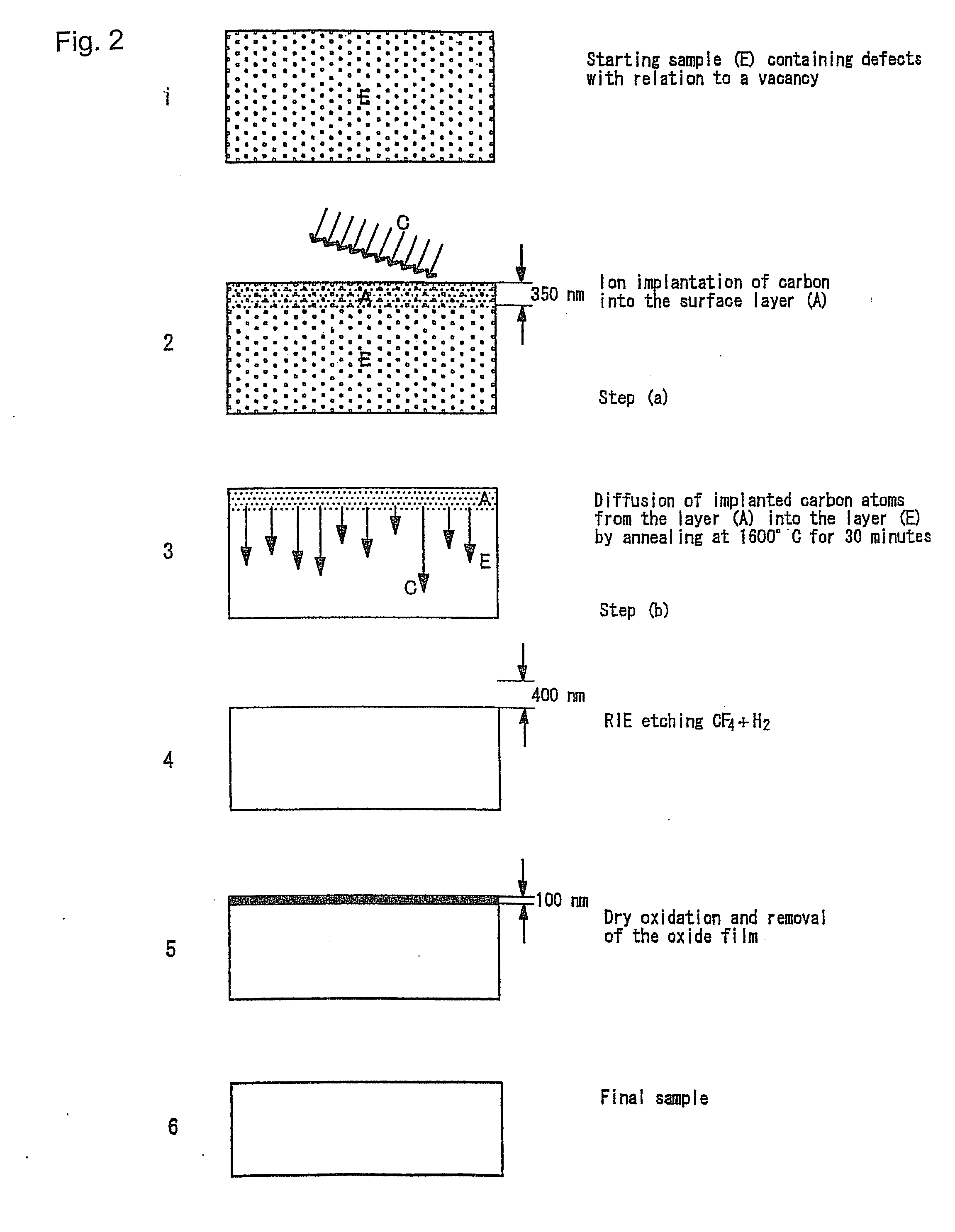
[0233]A preferred embodiment of the present invention will be described below in detail with reference to the accompanying drawings. FIG. 1 is a schematic view showing the process of fabricating an SiC layer in which recombination centers are reduced while utilizing the method according to a preferred embodiment of the present invention.

[0234]In the SiC crystal layer according to the present embodiment, an epitaxial layer (E) is grown from the surface of an SiC substrate (S). A known method, preferably chemical vapor deposition (CVD), is applied to the growth of the epitaxial layer (E).

[0235]As the step (a), carbon atoms (C) are ion-implanted into a shallow surface layer (A) of the epitaxial layer (E). By the above step, excess carbon interstitials are introduced into the surface layer (A).

[0236]Next, as the step (b), by heating the SiC crystal layer, carbon interstitials introduced into the surface layer (A) are diffused out from the surface layer (A) to the epitaxial layer (E) tha...


PUM


Abstract

A method for improving the quality of a SiC layer by effectively reducing or eliminating the carrier trapping centers by high temperature annealing and a SiC semiconductor device fabricated by the method. The method for improving the quality of a SiC layer by eliminating or reducing some carrier trapping centers includes the steps of: (a) carrying out ion implantation of carbon atom interstitials (C), silicon atoms, hydrogen atoms, or helium atoms into a shallow surface layer (A) of the starting SiC crystal layer (E) to introduce excess carbon interstitials into the implanted surface layer, and (b) heating the layer for making the carbon interstitials (C) to diffuse out from the implanted surface layer (A) into a bulk layer (E) and for making the electrically active point defects in the bulk layer inactive. After the above steps, the surface layer (A) can be etched or mechanically removed. The SiC semiconductor device is fabricated by the method.

Description

CROSS REFERENCE TO RELATED APPLICATION[0001]This application is a division of co-pending U.S. patent application Ser. No. 11 / 595,232 filed Nov. 10, 2006, entitled “Method for Improving the Quality of an SiC Crystal and an SiC Semiconductor Device” which is incorporated herein by reference in its entirety.BACKGROUND OF THE INVENTION[0002]1. Field of the Invention[0003]The present invention relates to a method for improving the quality of a crystal layer of SiC after the growth thereof. This invention also relates to a semiconductor device produced by carrying out such a method.[0004]2. Description of the Related Art[0005]FIG. 19 is a schematic view showing the atomic arrangement of Si and C in the perfect 4H-SiC crystal. The crystal lattices of semiconductors are not perfect even in the case where they do not contain any impurities, some amount of vacancies and interstitials is always present to maintain the thermodynamic equilibrium. As shown in FIG. 20, the point defects in a compo...

Claims


Application Information

Patent Timeline
Patent Type & Authority Applications(United States)
IPC IPC(8): H01L29/15
CPCC30B29/36C30B31/22H01L29/16H01L21/0445H01L29/7325H01L29/7395H01L21/322H01L29/1608H01L21/70
Inventor TSUCHIDA, HIDEKAZUSTORASTA, LIUTAURAS
Owner CENTRAL RESEARCH INSTITUTE OF ELECTRIC POWER INDUSTRY
Why Eureka
Try Eureka