

Semiconductor device and method for fabricating the same
a technology of semiconductor devices and insulating films, which is applied in the direction of semiconductor devices, electrical devices, transistors, etc., can solve the problems of difficult to stably secure the reliability of gate insulating films, degrading tbd (time to breakdown), etc., and achieves high reliability, high reliability, and stable security.
- Summary
- Abstract
- Description
- Claims
- Application Information
AI Technical Summary
Benefits of technology
Problems solved by technology
Method used
Image

Examples
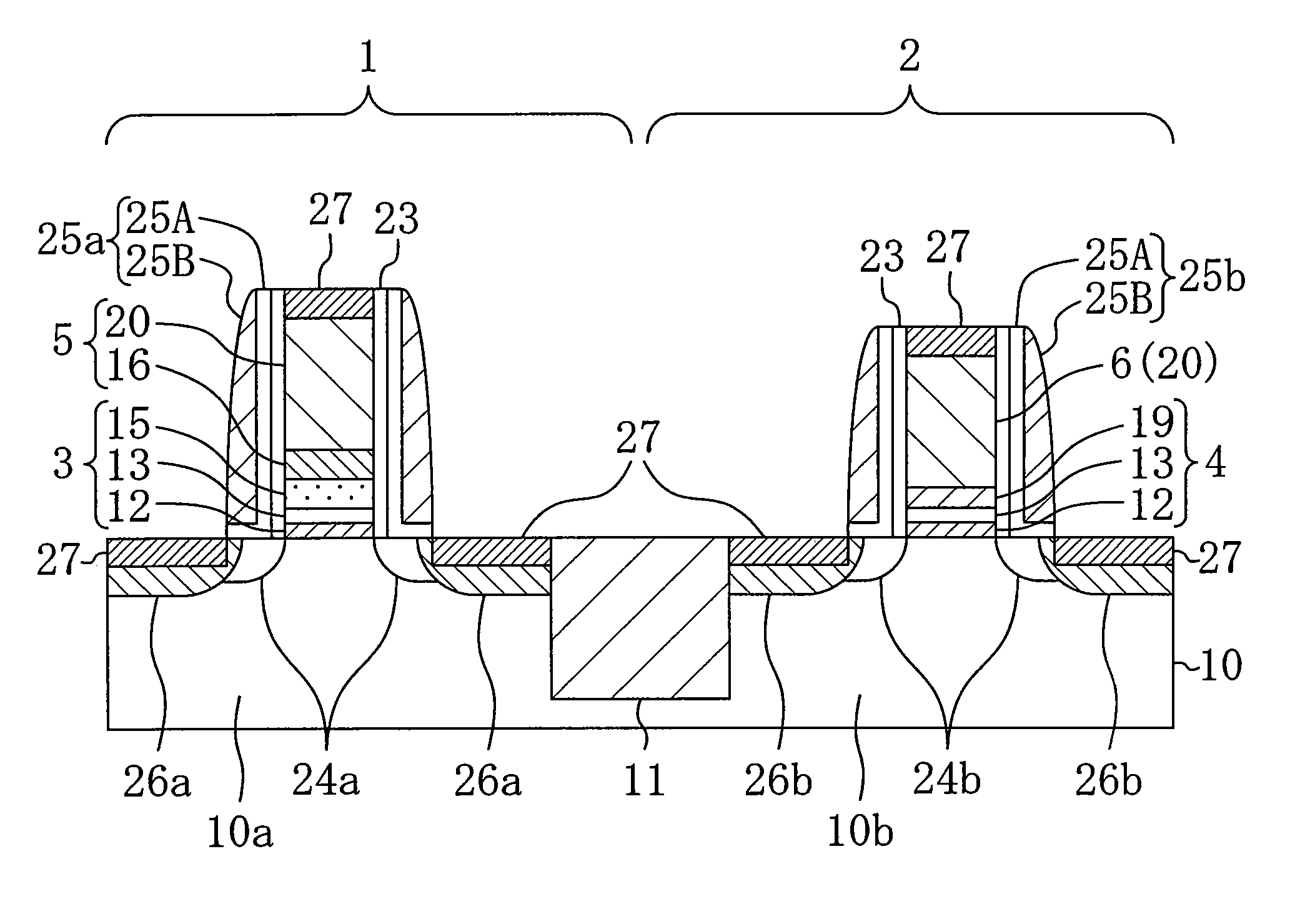
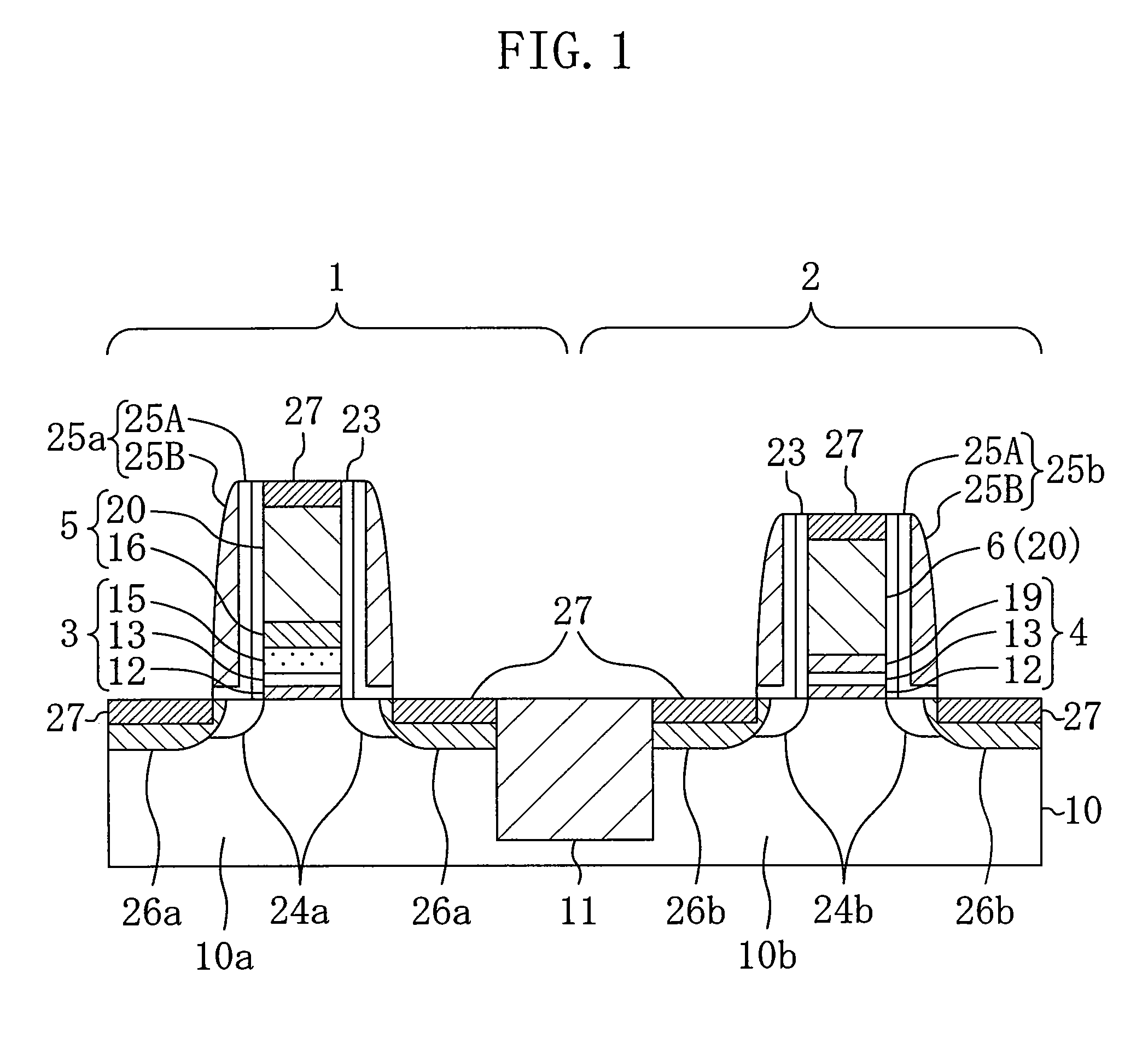
embodiment 1
Modification of Embodiment 1
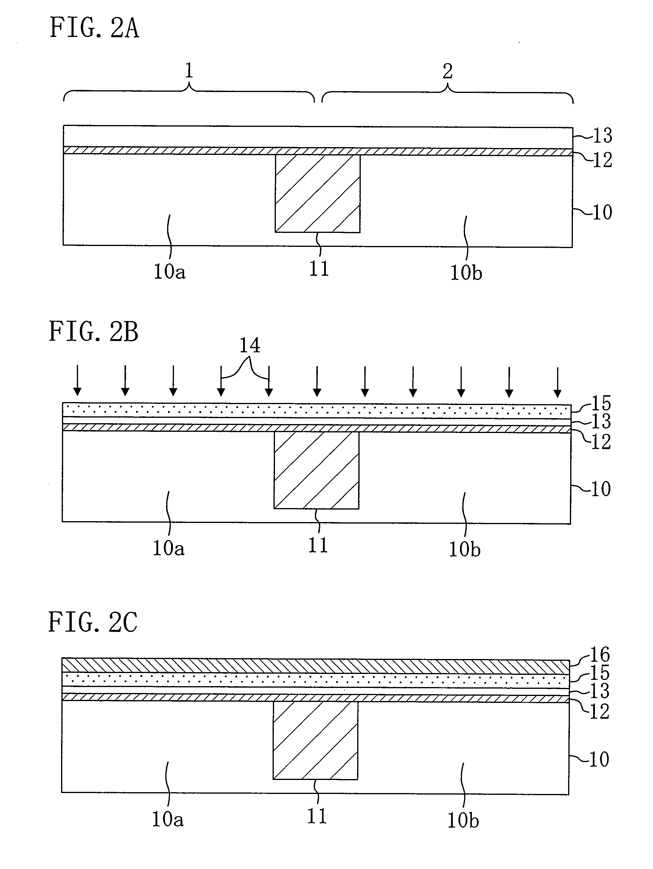
[0069]A semiconductor device and a method for fabricating the same according to a modification of Embodiment 1 of the invention will now be described with reference to the accompanying drawings.
[0070]FIGS. 5A and 5B are cross-sectional views for showing procedures in the method for fabricating a semiconductor device of this modification.
[0071]This modification is different from Embodiment 1 as follows: In Embodiment 1, the polysilicon film 20 is formed over the top face of the semiconductor substrate 10 so as to be in contact with the top faces of the TiN film 16 and the HfSiON modified layer 19 in the procedure of FIG. 3C. On the contrary, in this modification, a TaN film 30 with a thickness of 10 nm is formed by, for example, the PVD over the top face of the semiconductor substrate 10 so as to be in contact with the top faces of the TiN film 16 and the HfSiON modified layer 19 as shown in FIG. 5A, and thereafter, a polysilicon film 20 doped with, for ex...
embodiment 2
Modification of Embodiment 2
[0098]A semiconductor device and a method for fabricating the same according to a modification of Embodiment 2 of the invention will now be described with reference to the accompanying drawings.
[0099]FIGS. 10A and 10B are cross-sectional views for showing procedures in the method for fabricating a semiconductor device of this modification.
[0100]This modification is different from Embodiment 2 as follows: In Embodiment 2, the polysilicon film 20 is formed over the top face of the semiconductor substrate 10 so as to be in contact with the top faces of the TiN film 16 and the HfO2 modified layer 59 in the procedure of FIG. 8C. On the contrary, in this modification, a TaN film 30 with a thickness of 10 nm is formed by, for example, the PVD over the top face of the semiconductor substrate 10 so as to be in contact with the top faces of the TiN film 16 and the HfO2 modified layer 59, and thereafter, a polysilicon film 20 doped with, for example, an N-type impur...
PUM
 Abstract
Description
Claims
Application Information