Circuit member, manufacturing method for circuit members, semiconductor device, and surface lamination structure for circuit member

a manufacturing method and circuit technology, applied in the field of circuit members, can solve the problems of difficult to expect a great effect with respect to the adhesion of insulating resins in packages, takes time for etching, and little effective surface roughing of rolled copper plates, etc., to achieve greater surface roughness and reduce the effect of roughness

Active Publication Date: 2009-02-12
DAI NIPPON PRINTING CO LTD
View PDF14 Cites 82 Cited by
  • Summary
  • Abstract
  • Description
  • Claims
  • Application Information

AI Technical Summary

Benefits of technology

[0011]It therefore is a main object of the present invention to provide a lead frame allowing for enhancement of adhesion strength to a sealing resin, and a manufacturing method of the same, as well as a semiconductor device.
[0013]It is still another object of the present invention to provide a surface lamination structure for a circuit member allowing for enhancement of adhesion strength to a sealing resin.

Problems solved by technology

However, the etching solution of organic acid system in the above-noted patent material-1 is effective to a copper surface formed by a plating method, but is little effective for roughing surfaces of a rolled copper plate that is a substrate of lead frame, as a problem.
Hence, for lead frames treated for roughing with an etching solution of organic acid system, it was difficult to expect a great effect with respect to the adhesion to an insulating resin constituting a package.
Such a treating method thus takes time for etching, and has not been adaptive for production a practical lead frame.

Method used


Image

  • Circuit member, manufacturing method for circuit members, semiconductor device, and surface lamination structure for circuit member
  • Circuit member, manufacturing method for circuit members, semiconductor device, and surface lamination structure for circuit member
  • Circuit member, manufacturing method for circuit members, semiconductor device, and surface lamination structure for circuit member

Examples


first embodiment

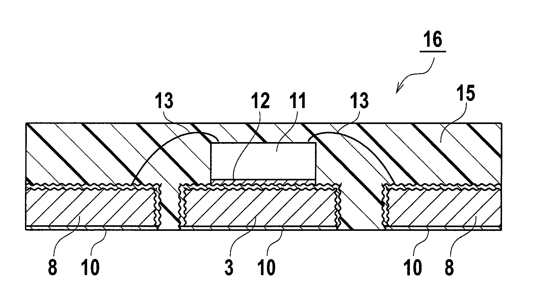
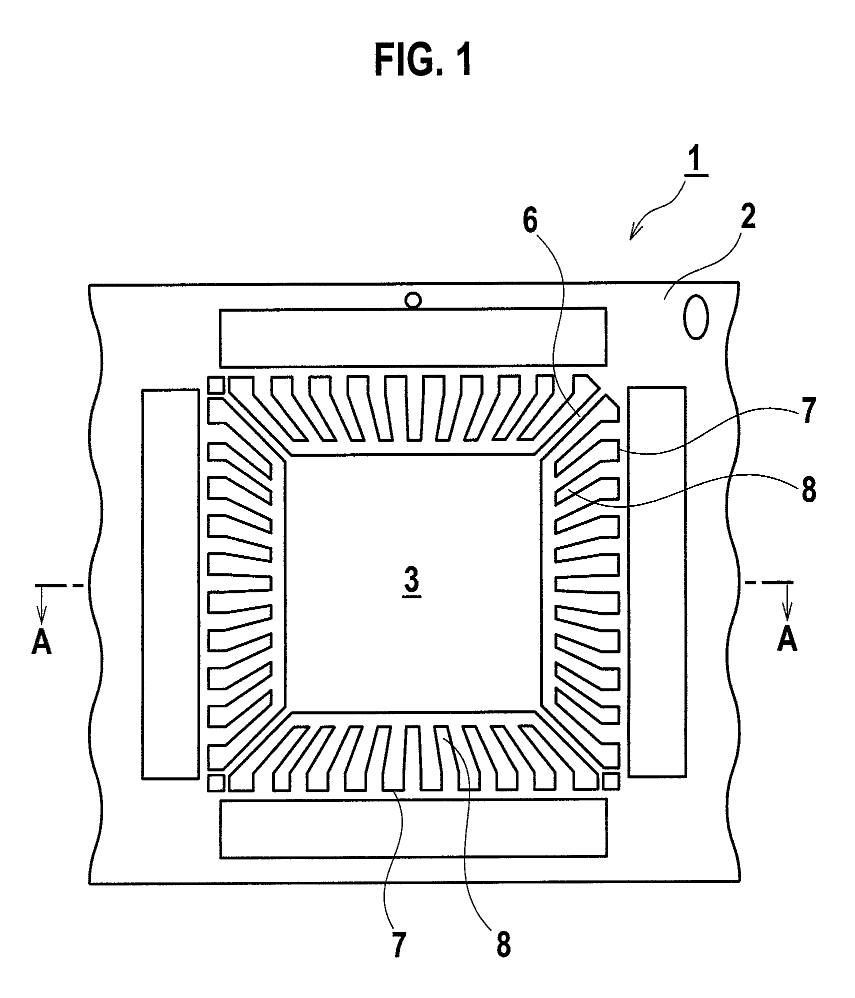
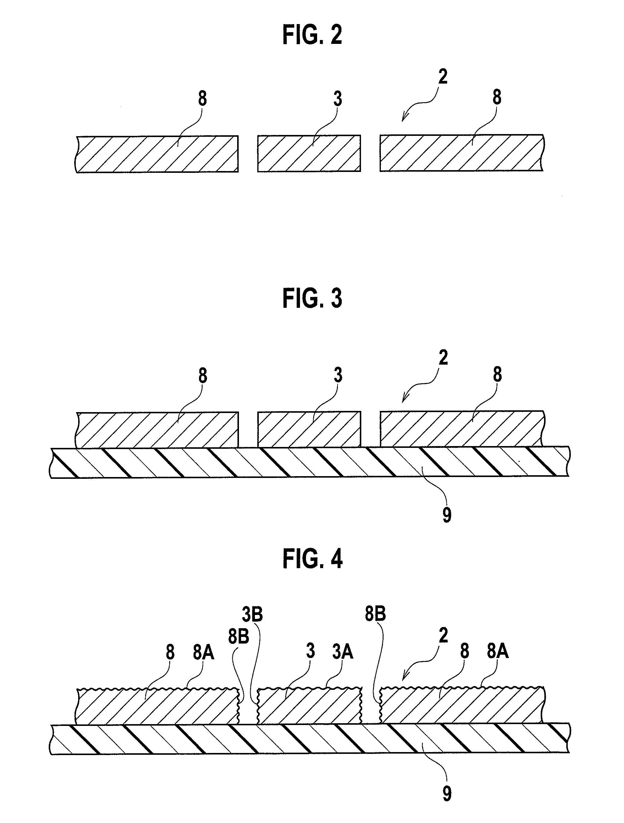
[0041]FIG. 1 to FIG. 9 show a fi embodiment of the present invention. FIG. 1 is a plan view of a lead frame, and FIG. 2 to FIG. 9 illustrate processes in a manufacturing method of the lead frame, as well as of a semiconductor device, with respect to a section A-A of FIG. 1.

[0042](Configuration of Lead Frame)

[0043]According to the present embodiment, a lead frame 1 is manufactured in the form of a frame substrate 2 as a rolled copper plate or rolled copper alloy plate of an elongate ribbon shape that is patterned by, among others, an etching or a die-blanking, to have a plurality of consecutive unit patterns. It is noted that FIG. 1 shows a single unit pattern in the lead frame 1.

[0044]As shown in FIG. 1, the unit pattern of lead frame 1 has a die pad portion 3 formed, in a central region, in a rectangular shape for a semiconductor chip to be mounted thereon, a set of lead portions 8 formed so as to surround the die pad portion 3, a set of tie bars 6 linking the die pad portion 3 wit...

second embodiment

[0067]Description is now made of a second embodiment of the present invention, with reference to FIG. 12 and FIG. 13. It is noted that in this embodiment, like parts to the first embodiment are designated by like reference characters, for elimination of redundancy.

[0068]According to the second embodiment, for a lead frame as a circuit member, those surface portions to be brought into contact with a resin sealing mold are made smooth, and the remaining surface portions are roughed, to effect prevention of resin leakage and occurrences of resin burrs when molding the sealing resin. FIG. 12(a) shows a section of a frame substrate 2 patterned like FIG. 2. For the partial roughing, as shown in FIG. 12(b), instead of the method of laminating a protecting film on a downside of a frame substrate 2 described with reference to FIG. 3, there is employed a method of pinching a frame substrate 2 by a pair of upper and lower etching jigs 29 and 30, with rubber packing elements 27 and 28 put in be...

third embodiment

[0075]Description is now made of a circuit member according to a third embodiment of the present invention, with reference to FIG. 15 and FIG. 16. It is noted that in this embodiment, like parts to the first embodiment are designated by like reference characters, for elimination of redundancy.

[0076]This embodiment provides in advance a frame substrate 2 shown in FIG. 15(a), which is made of a rolled copper alloy, and has a prescribed pattern of lead frame formed thereon, including a die pad portion 3, lead portions 8, etc., by an etching or die-blanking.

[0077]Next, as shown in FIG. 15 (b), precious-metal skins 10B are plated on a semiconductor chip mounting portion of a die pad upside surface and on bonding wire connecting portions of lead upside surfaces of the frame substrate 2, and as shown in FIG. 15(c), a protecting (masking material) film 9 is laminated on a downside of the frame substrate 2.

[0078]Next, a micro-etching solution is injected over surfaces of the frame substrate ...


PUM

PropertyMeasurementUnit
Raaaaaaaaaaa
thicknessaaaaaaaaaa
thicknessaaaaaaaaaa

Abstract

A circuit member includes a frame substrate formed, by patterning a rolled copper plate or a rolled copper alloy plate, with a die pad portion for a semiconductor chip to be mounted thereon, and a lead portion for an electrical connection to the semiconductor chip, having rough surfaces formed as roughed surfaces on upsides and lateral wall sides of the die pad portion and the lead portion, and smooth surfaces formed on downsides of the die pad portion and the lead portion, and the die pad portion and the lead portion are buried in a sealing resin, having a downside of the lead portion exposed.

Description

TECHNICAL FIELD[0001]The present invention is addressed among others to a lamination structure for circuit member surfaces, and a surface treating technique for a lead frame as a circuit member, as well as a semiconductor device using the circuit member, and particularly, to a technique for enhancement of strength in adhesion between a lead frame and a sealing resin in accordance with a type of semiconductor package.BACKGROUND ART[0002]The semiconductor device may be a semiconductor package with a structure having a semiconductor chip, such as an IC chip or LSI chip, mounted on a lead frame, and sealed with an insulating resin. For such semiconductor devices, along with advancements in high-integration and miniaturization, their package structures have developed through such types that had an external lead projecting out of a lateral wall of a resin package, as in an SOJ (small outline J-leaded package) and a QFP (quad flat package), to such types that have an external lead buried f...

Claims


Application Information

Patent Timeline
Patent Type & Authority Applications(United States)
IPC IPC(8): H01L23/495H05K3/10H05K3/30
CPCH01L21/561H01L21/565H01L21/568H01L23/3107H01L23/3142H01L23/49548H01L23/49582H01L24/32H01L24/48H01L24/97H01L2224/05647H01L2224/32057H01L2224/32245H01L2224/48091H01L2224/48247H01L2224/484H01L2224/73265H01L2224/83385H01L2224/85385H01L2224/85439H01L2224/85444H01L2224/85447H01L2224/85464H01L2224/97H01L2924/01002H01L2924/01004H01L2924/01005H01L2924/01028H01L2924/01029H01L2924/01033H01L2924/01046H01L2924/01047H01L2924/0105H01L2924/01057H01L2924/01078H01L2924/01079H01L2924/01082H01L2924/01088H01L2924/014H01L2924/14H01L2924/18301H01L2924/00014H01L2924/01006H01L2924/01023H01L2924/0132H01L2924/10253Y10T29/49121Y10T29/49155Y10T29/4913Y10T29/49124H01L2224/85H01L2224/83H01L2224/45099H01L2924/00012H01L2924/00H01L24/73H01L2924/15747H01L2924/181H01L23/02H01L23/50
Inventor SHIMAZAKI, YOSAITO, HIROYUKIMASUDA, MASACHIKAMATSUMURA, KENJIFUKUCHI, MASARUIKEZAWA, TAKAO
Owner DAI NIPPON PRINTING CO LTD
Why Eureka
Try Eureka