Increased nanosecond laser pulse-to-pulse energy repeatability using active laser pulse energy control

a laser pulse and pulse energy control technology, applied in lasers, laser beam welding apparatus, manufacturing tools, etc., can solve the problems of limited heat dissipation into surrounding space or structures, heat cannot be easily dissipated, and the entire wafer is heated, so as to reduce the variation increase the repeatability of pulse-to-pulse laser energy

Inactive Publication Date: 2009-02-19
APPLIED MATERIALS INC
View PDF5 Cites 5 Cited by
  • Summary
  • Abstract
  • Description
  • Claims
  • Application Information

AI Technical Summary

Benefits of technology

[0011]Embodiments of the present invention generally relate to reducing the pulse-to-pulse laser energy variation (i.e., increasing the pulse-to-pulse laser energy repeatability) from a pulsed laser source.

Problems solved by technology

A drawback of RTP processes is that they heat the entire wafer even though the IC devices typically reside only in the top few microns of the silicon wafer.
This limits how fast one can heat up and cool down the wafer.
Moreover, once the entire wafer is at an elevated temperature, heat can only dissipate into the surrounding space or structures.
As a result, today's state of the art RTP systems struggle to achieve a 400° C. / s ramp-up rate and a 150° C. / s ramp-down rate.
While RTP and spike annealing processes are widely used, current technology is not ideal, and tends to ramp the wafer temperature during thermal processing too slowly and thus expose the wafer to elevated temperatures for too long a period of time.
These thermal budget type problems become more severe with increasing wafer sizes, increasing switching speeds, and / or decreasing feature sizes.
Due to the stringent uniformity requirements and the complexity of minimizing the overlap of scanned regions across the substrate surface these types of processes are not effective for thermal processing contact level devices formed on the surface of the substrate.
Due to the shrinking semiconductor device sizes and stringent device processing characteristics the tolerance in the variation in the amount of energy delivered during each pulse to different devices formed on the substrate surface is very low.
This pump is not well-controlled in the Q-switched laser, and therefore, these conventional pulsed laser sources typically perform with an unacceptable pulse-to-pulse energy variation on the order of 10%.

Method used


Image

  • Increased nanosecond laser pulse-to-pulse energy repeatability using active laser pulse energy control
  • Increased nanosecond laser pulse-to-pulse energy repeatability using active laser pulse energy control
  • Increased nanosecond laser pulse-to-pulse energy repeatability using active laser pulse energy control

Examples


Embodiment Construction

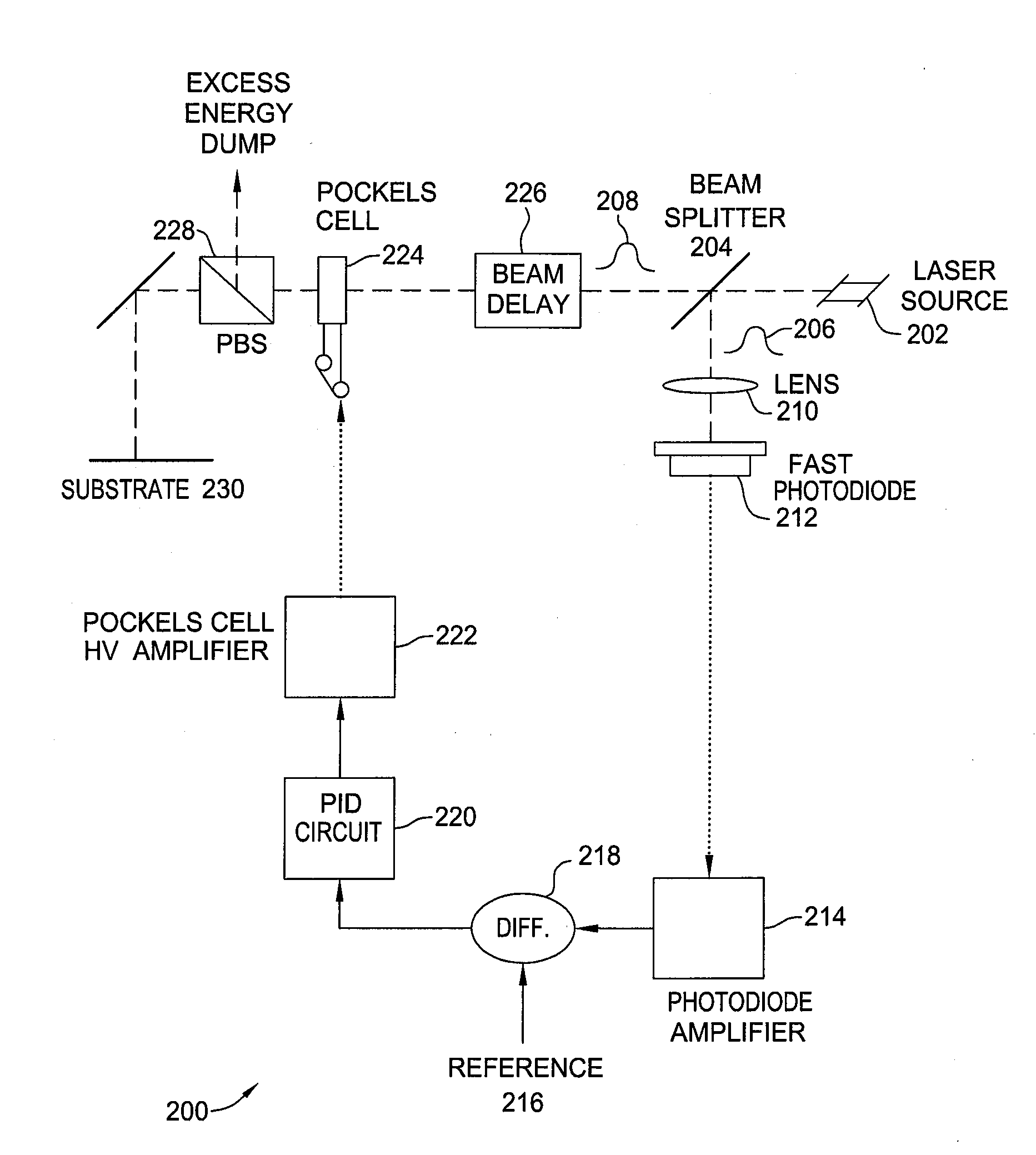
[0025]Embodiments of the present invention provide techniques and apparatus for reducing the pulse-to-pulse laser energy variation (i.e., increasing the pulse-to-pulse laser energy repeatability) from a pulsed laser source. In this manner, laser pulses impingent on a processing plane, such as the surface of a wafer or other substrate, may have substantially the same energy content leading to a more controlled annealing process when compared to conventional annealing. The technique may be based on in-situ detection of the pulse energy level and the subsequent active adjustment of the transmitted laser pulse energy in a closed-loop control scheme. Furthermore, the active adjustment of the energy in each laser pulse may occur within a few nanoseconds after the original laser pulse is generated by a pulsed laser source.

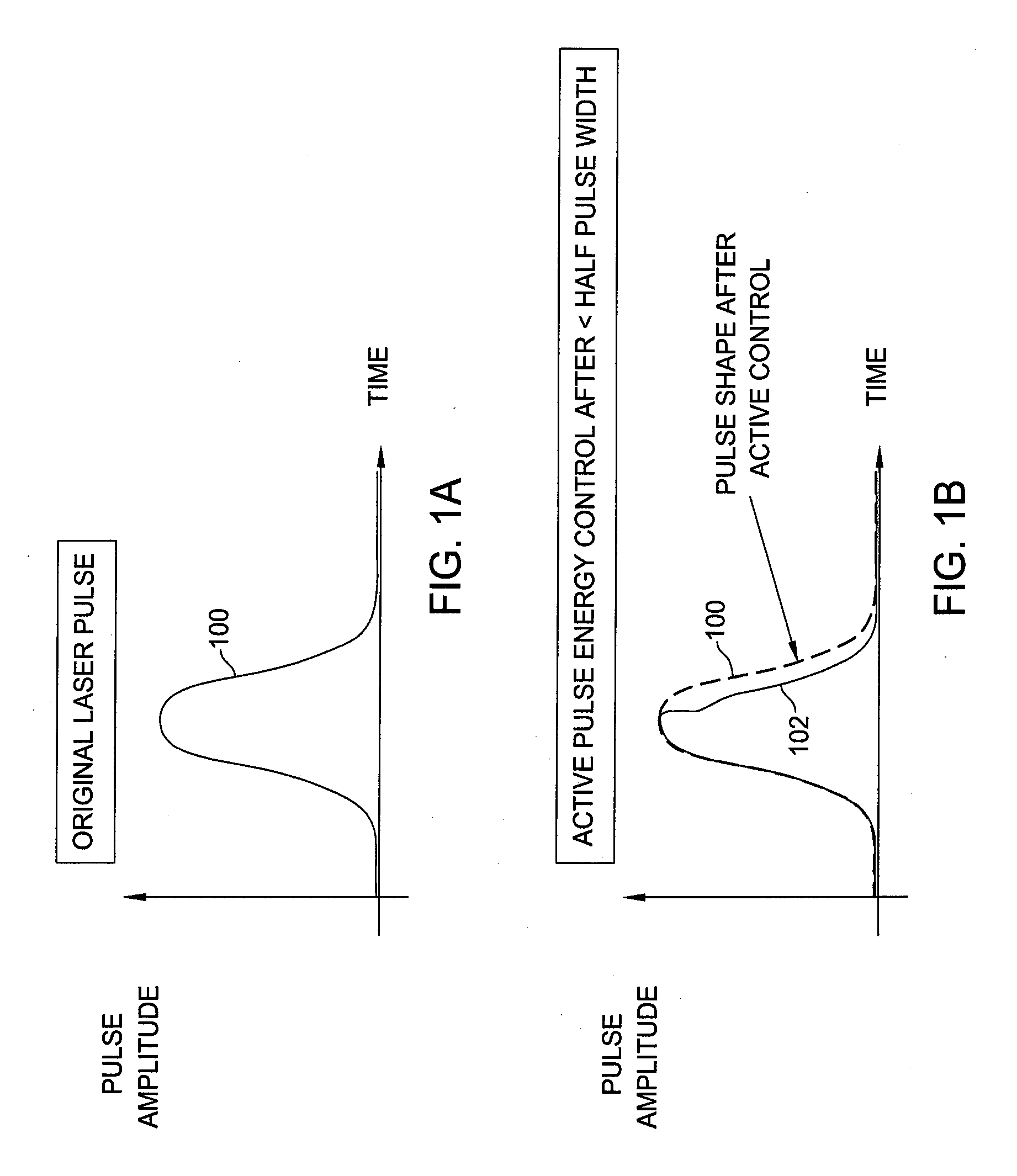
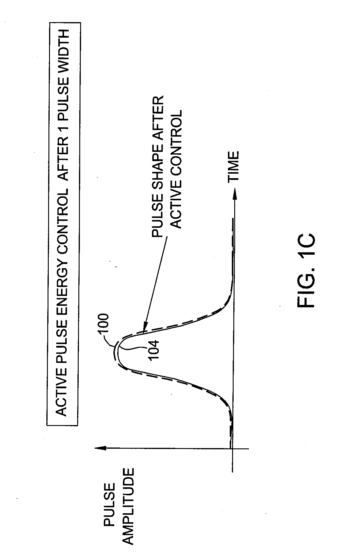
[0026]There may be a number of ways to actively control the energy content of a transmitted laser pulse. FIG. 1A illustrates an exemplary, Gaussian laser pulse 100 origin...


PUM

PropertyMeasurementUnit
frequencyaaaaaaaaaa
wavelengthaaaaaaaaaa

Abstract

A method and apparatus for reducing the pulse-to-pulse laser energy variation (i.e., increasing the pulse-to-pulse laser energy repeatability) from a pulsed laser source are provided. In this manner, laser pulses impingent on a processing plane, such as the surface of a wafer or other substrate, may have substantially the same energy content leading to a more controlled process when compared to conventional processing. The method may be based on in-situ detection of the pulse energy level and the subsequent active adjustment of the transmitted laser pulse energy in a closed-loop control scheme. Furthermore, the active adjustment of the laser pulse energy may occur within a few nanoseconds after the original laser pulse is generated by a pulsed laser source.

Description

BACKGROUND OF THE INVENTION[0001]1. Field of the Invention[0002]Embodiments of the present invention generally relate to laser annealing and, more particularly, to a method of reducing the pulse-to-pulse laser energy variation from a pulsed laser source.[0003]2. Description of the Related Art[0004]The integrated circuit (IC) market is continually demanding greater memory capacity, faster switching speeds, and smaller feature sizes. One of the major steps the industry has taken to address these demands is to change from batch processing silicon wafers in large furnaces to single wafer processing in a small chamber.[0005]During such single wafer processing the wafer is typically heated to high temperatures so that various chemical and physical reactions can take place in multiple IC devices defined in the wafer. Of particular interest, favorable electrical performance of the IC devices requires implanted regions to be annealed. Annealing recreates a more crystalline structure from reg...

Claims


Application Information

Patent Timeline
Patent Type & Authority Applications(United States)
IPC IPC(8): H01S3/10
CPCH01L21/2026B23K26/063B23K26/0622H01L21/02686
Inventor LI, JIPINGTHOMAS, TIMOTHY N.JENNINGS, DEANADAMS, BRUCE E.HUNTER, AARON MUIR
Owner APPLIED MATERIALS INC
Why Eureka
Try Eureka