Layered-filament lattice for chemical mechanical polishing

a technology of chemical mechanical polishing and layers, which is applied in the direction of lapping tools, grinding/polishing apparatuses, manufacturing tools, etc., can solve the problems of clogging the surface voids as well as the debris affecting the uniformity of the polishing between wafers or within wafers, and reducing the polishing rate of the cmp process

Active Publication Date: 2009-02-19
ROHM & HAAS ELECTRONICS MATERIALS CMP HLDG INC
View PDF17 Cites 14 Cited by
  • Summary
  • Abstract
  • Description
  • Claims
  • Application Information

AI Technical Summary

Benefits of technology

[0014]An embodiment of the invention provides a polishing pad useful for polishing at least one of a magnetic, optical and semiconductor substrate in the presence of a polishing medium, comprising multiple layers of polishing filaments stacked on a base layer of polishing filaments, the multiple layers of polishing filaments having a sequential stacked formation with each layer of the polishing filam...

Problems solved by technology

Additionally, debris from the CMP process can clog the surface voids as well as the micro-channels through which slurry flows across the polishing surface.
When this occurs, the polishing rate of the CMP process decreases, and this can result in non-uniform polishing between wafers or within a wafer.
Although pad designers have produced various microstructures and configurations of surface texture through both pad material preparation and surface conditioning, existing CMP pad polishing textures are less than optimal in two important aspects.
First, the actual contact area between a conventional CMP pad and a typical workpiece under the applied pressures practiced in CMP is small-usually only a few percent of the total confronting area.
This is a direct consequence of the inexactness of conventional surface conditioning that amounts to randomly tearing the solid regions of the structure into tatters, leaving a population of features, or asperities, of various shapes and heights of which only the tallest actually contact the workpiece.
Second, the space available for slurry flow to convey away polish debris and heat occupies a thin layer at the pad surface such that polishing waste remains in close proximity with the workpiece until it passes completely out from under the workpiece.
This results in a high probability that the workpiece is re-exposed to both spent chemistry and material previously removed.
Thu...

Method used


Image

  • Layered-filament lattice for chemical mechanical polishing
  • Layered-filament lattice for chemical mechanical polishing
  • Layered-filament lattice for chemical mechanical polishing

Examples


Embodiment Construction

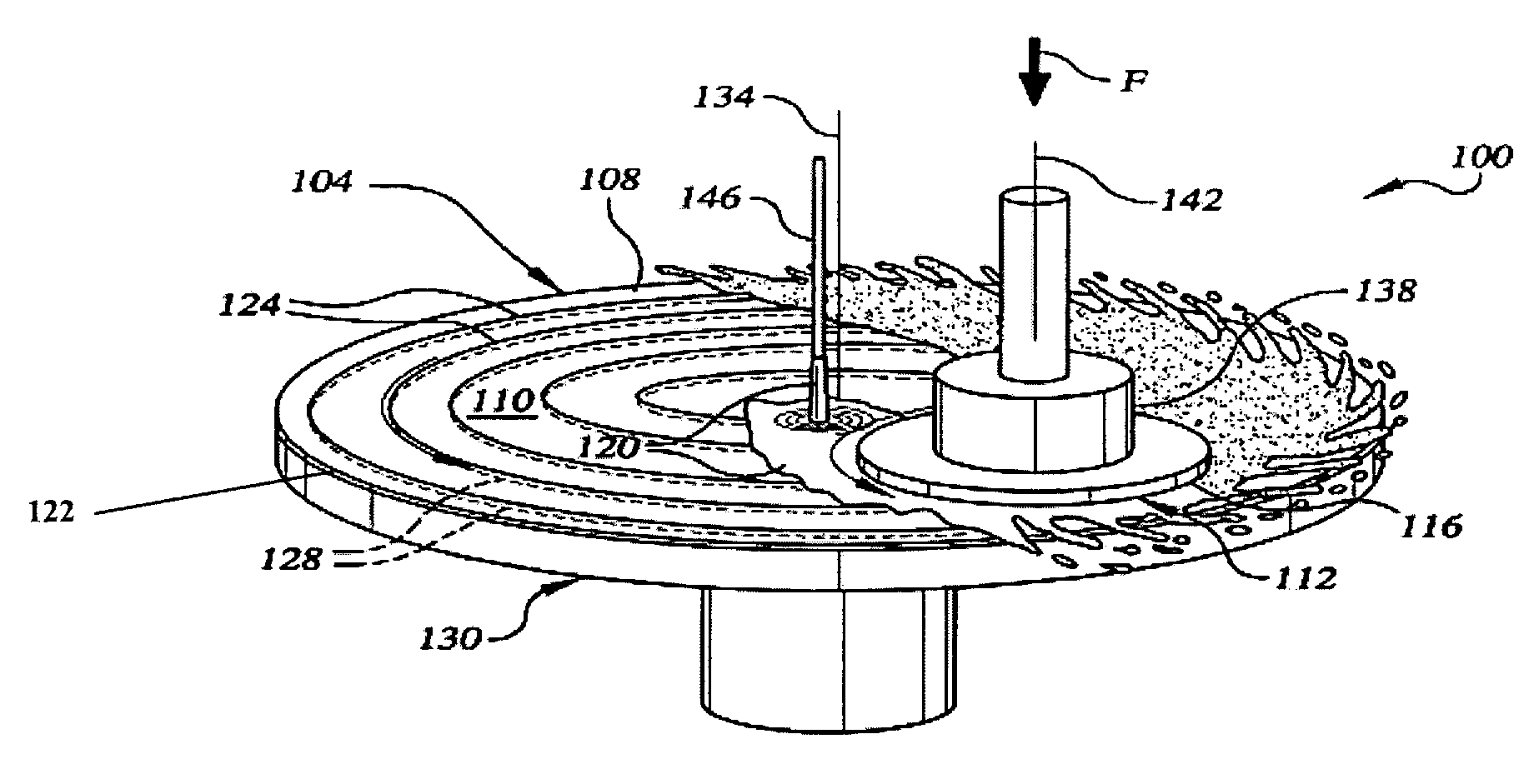
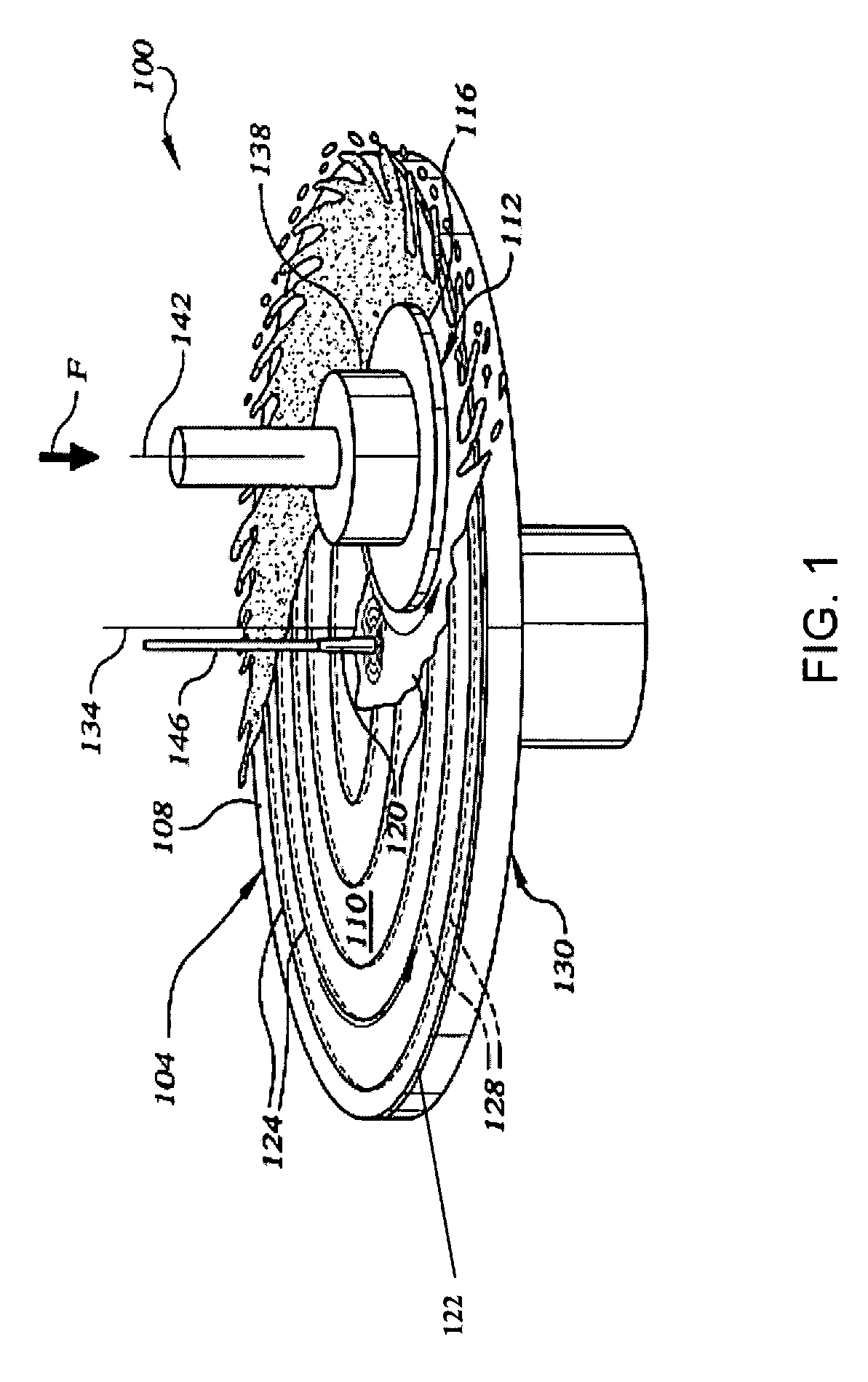
[0024]Referring to the drawings, FIG. 1 generally illustrates the primary features of a dual-axis chemical mechanical polishing (CMP) polisher 100 suitable for use with a polishing pad 104 of the present invention. Polishing pad 104 generally includes a polishing layer 108 having a polishing surface 110 for confronting an article, such as semiconductor wafer 112 (processed or unprocessed) or other workpiece, e.g., glass, flat panel display or magnetic information storage disk, among others, so as to effect polishing of the polished surface 116 of the workpiece in the presence of a polishing medium 120. Polishing medium 120 travels to polishing pad perimeter 122 through optional spiral groove 124 having a depth 128. For the sake of convenience, the term “wafer” is used below without the loss of generality. In addition, as used in this specification, including the claims, the term “polishing medium” includes particle-containing polishing solutions and non-particle-containing solutions...


PUM

PropertyMeasurementUnit
Fractionaaaaaaaaaa
Fractionaaaaaaaaaa
Widthaaaaaaaaaa

Abstract

The polishing pad (104) is useful for polishing at least one of a magnetic, optical and semiconductor substrate (112) in the presence of a polishing medium (120). The polishing pad 104 includes multiple layers of polishing filaments (200, 300, 400, 500) stacked on a base layer (204, 404, 504) of polishing filaments, the multiple layers of polishing filaments (200, 300, 400, 500) having a sequential stacked formation with each layer of the polishing filaments being above and attached to a lower polishing filament, the multiple layers of polishing filaments (200, 300, 400, 500) being parallel to a polishing surface of the polishing pad (104) and wherein individual polishing filaments (202, 302, 402) of the multiple layers of polishing filaments (200, 300, 400, 500) are above an average of at least three polishing filaments (202, 302, 402), to form the polishing pad having an open lattice structure of interconnected polishing filaments (210, 310, 410, 510, 610).

Description

BACKGROUND OF THE INVENTION[0001]The present invention relates generally to the field of polishing pads for chemical mechanical polishing. In particular, the present invention is directed to a chemical mechanical polishing pad having a polishing structure useful for chemical mechanical polishing magnetic, optical and semiconductor substrates.[0002]In the fabrication of integrated circuits and other electronic devices, multiple layers of conducting, semiconducting and dielectric materials are deposited onto and removed from a surface of a semiconductor wafer. Thin layers of conducting, semiconducting and dielectric materials may be deposited using a number of deposition techniques. Common deposition techniques in modern wafer processing include physical vapor deposition (PVD), also known as sputtering, chemical vapor deposition (CVD), plasma-enhanced chemical vapor deposition (PECVD) and electrochemical plating, among others. Common removal techniques include wet and dry isotropic an...

Claims


Application Information

Patent Timeline
IPC IPC(8): B24B29/02
CPCB24B37/22B24D11/00H01L21/304
Inventor MULDOWNEY, GREGORY P.
Owner ROHM & HAAS ELECTRONICS MATERIALS CMP HLDG INC
Why Eureka
Try Eureka