Semiconductor memory device and method of manufacturing the same

a memory device and semiconductor technology, applied in the direction of semiconductor devices, basic electric elements, electrical appliances, etc., can solve problems such as program disturbance and become problems

Inactive Publication Date: 2009-02-26
RENESAS TECH CORP
View PDF2 Cites 63 Cited by
  • Summary
  • Abstract
  • Description
  • Claims
  • Application Information

AI Technical Summary

Benefits of technology

[0015]In a split gate type MONOS memory cell, it is possible to improve the disturb tolerance at the time of program by the SSI method, without reducing a read current. Further, because the disturb tolerance of the unselected memory cell is improved, it is possible to reduce the area of the memory module.

Problems solved by technology

When program is performed by the SSI method, in the split gate type MONOS memory cell, a program disturb becomes a problem.
Therefore, there are unselected memory cells to which the high voltage of program is applied in both the source regions and the memory gate electrodes, and in the unselected memory cells, weak program in which electrons are injected into the charge accumulation region occurs, which becomes a problem.

Method used


Image

  • Semiconductor memory device and method of manufacturing the same
  • Semiconductor memory device and method of manufacturing the same
  • Semiconductor memory device and method of manufacturing the same

Examples


first embodiment

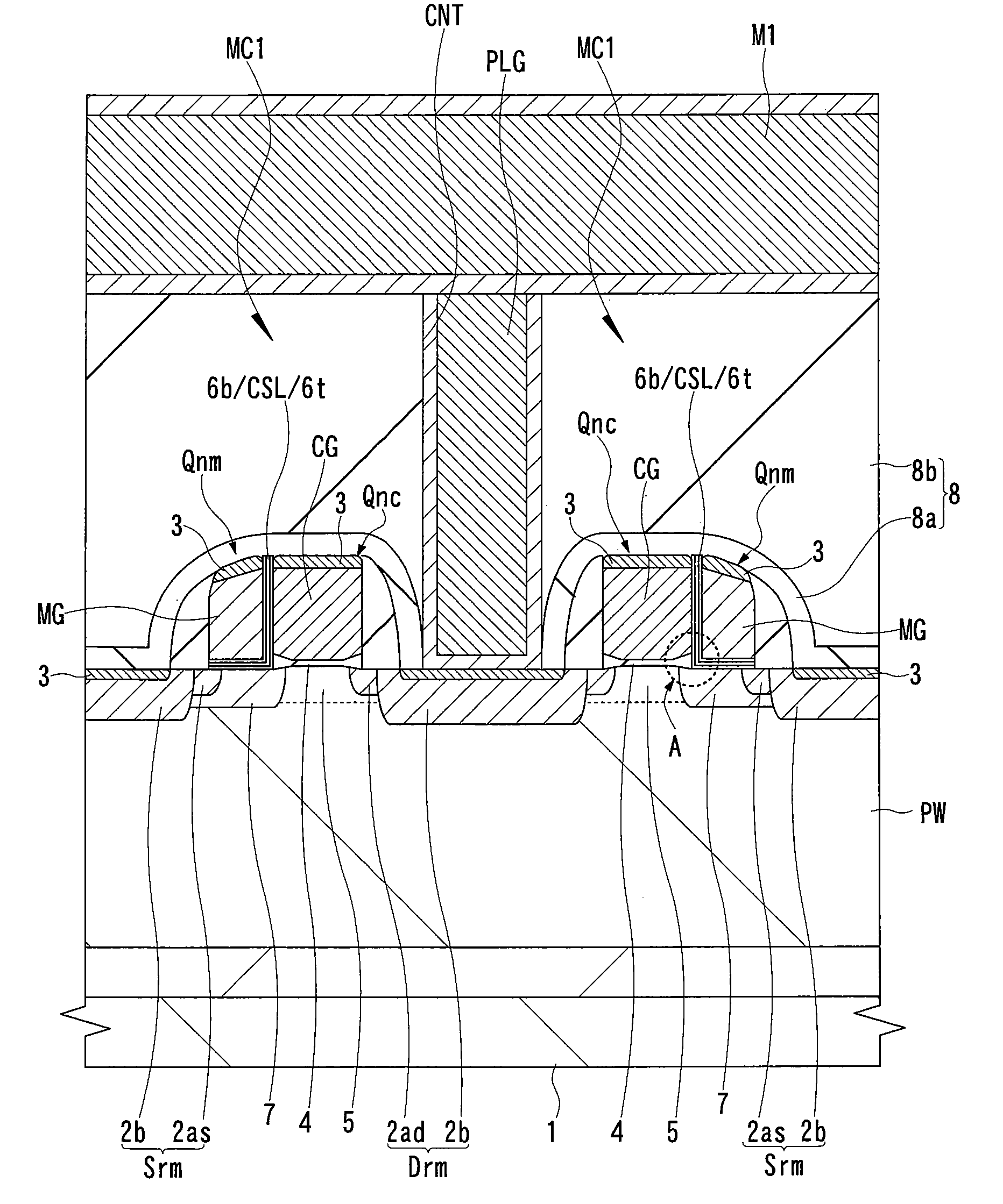
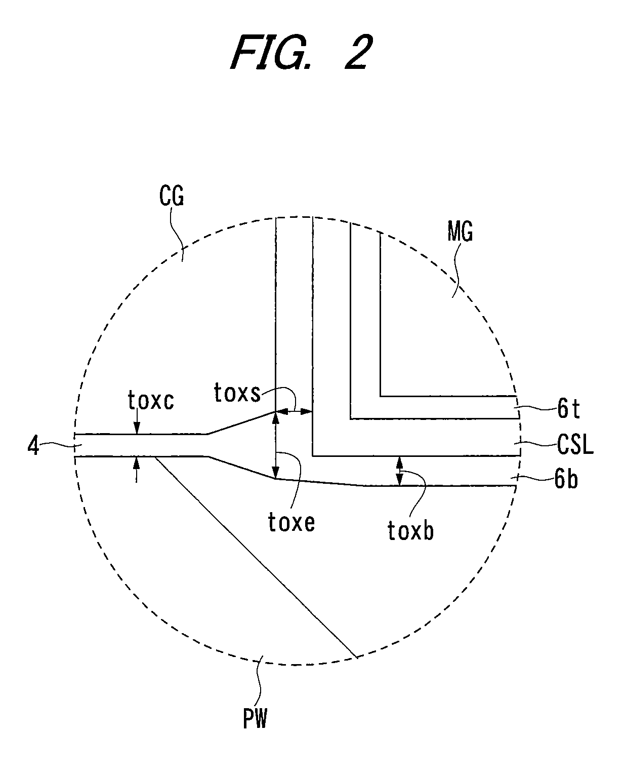
[0058]An example of the structure of a split gate type MONOS memory cell according to a first embodiment of the present invention will be explained with reference to FIGS. 1 and 2. FIG. 1 is a cross sectional view showing the main part of a split gate type MONOS memory cell in which the channel is cut along the direction intersecting to its memory gate electrode, and FIG. 2 is an enlarged cross sectional view of a main part showing the region A of FIG. 1.

[0059]As shown in FIG. 1, a semiconductor substrate 1 is made of, for example, p-type single crystal silicon, a p well PW into which p-type impurities are included is formed. In the active region of the main surface (device formation surface) of the semiconductor substrate 1, an nMIS (Qnc) for selection and an nMIS (Qnm) for memory of a memory cell MC1 according to the first embodiment are arranged. The drain region Drm and the source region Srm of this memory cell MC1 have, for example, n−-type semiconductor regions 2ad and 2as wit...

second embodiment

[0121]In a second embodiment, an example of the method of manufacturing a split gate type MONOS memory cell in which the formation method of the gate dielectric of nMIS for select is different from that in the first embodiment mentioned above will be explained. The method of manufacturing a split gate type MONOS memory cell by the second embodiment will be explained with reference to FIGS. 22 to 24. FIGS. 22 to 24 are cross sectional views showing the main part of a memory cell in the process of manufacture of the semiconductor device. The array structure and the operation conditions of a split gate type MONOS memory cell according to the second embodiment are same as those in the first embodiment mentioned above. Incidentally, because the manufacturing processes except the process of forming the gate dielectric of the nMIS for select is similar to the manufacturing process of the memory cell MC1 of the first embodiment mentioned above, the explanation thereof is omitted herein.

[012...

third embodiment

[0126]In a third embodiment, an example of the method of manufacturing a split gate type MONOS memory cell in which the formation method of the gate dielectric of the nMIS for select is different from that in the first and second embodiments mentioned above will be explained. The method of manufacturing the split gate type MONOS memory cell according to the third embodiment will be explained with reference to FIGS. 25 to 28. FIGS. 25 to 28 are cross sectional views showing the main part of a memory cell in the process of manufacture of the semiconductor device. The array structure and the operation conditions of a split gate type MONOS memory cell according to the third embodiment are same as those in the first embodiment mentioned above. Incidentally, because the manufacturing processes except the process of forming the gate dielectric of the nMIS for select is similar to the manufacturing process of the memory cell MC1 of the first embodiment mentioned above, the explanation there...


PUM


Abstract

In a memory cell including an nMIS for memory formed on the sides of an nMIS for select and an nMIS for select via dielectric films and a charge storage layer, the thickness of a gate dielectric under the gate longitudinal direction end of a select gate electrode is formed thicker than that of the gate dielectric under the gate longitudinal direction center and the thickness of the lower layer dielectric film that is positioned between the select gate electrode and the charge storage layer and is nearest to a semiconductor substrate is formed 1.5 times or below of the thickness of the lower layer dielectric film positioned between the semiconductor substrate and the charge storage layer.

Description

CROSS-REFERENCE TO RELATED APPLICATION[0001]The present application claims priority from Japanese Patent Application No. JP 2007-218498 filed on Aug. 24, 2007, the content of which is hereby incorporated by reference into this application.TECHNICAL FIELD OF THE INVENTION[0002]The present invention relates to a semiconductor memory device and a technology of manufacturing the same, in particular, to a technology effective when applied to a semiconductor memory device having an MONOS (Metal Oxide Nitride Oxide Semiconductor) memory cell in which a nitride film is a charge storage layer.BACKGROUND OF THE INVENTION[0003]As a nonvolatile semiconductor memory device to which data can be written and erased electrically, an EEPROM (Electrical Erasable and Programmable Read Only Memory) is used now. In the memory cell of the nonvolatile semiconductor memory device represented by a flash memory, an charge accumulation region represented by a conductive floating gate electrode surrounded by an...

Claims


Application Information

Patent Timeline
Patent Type & Authority Applications(United States)
IPC IPC(8): H01L29/792H01L21/336
CPCH01L27/115H01L29/792H01L29/66833H01L27/11568H10B43/30H10B69/00H10B99/00
Inventor ISHIMARU, TETSUYAKAWASHIMA, YOSHIYUKISHIMAMOTO, YASUHIROYASUI, KANARIGANE, TSUYOSHIMINE, TOSHIYUKI
Owner RENESAS TECH CORP
Why Eureka
Try Eureka