Micro-power source module

a micro-power source module and micro-power source technology, applied in the direction of dc source parallel operation, continuous variable inductance/transformer, inductance, etc., can solve the problems of strict restrictions on the space of printed circuit boards, difficult to dispose of all and difficult to dispose of plural pol power sources close to an lsi. , to achieve the effect of reducing the noise that reaches the output terminal, small

Active Publication Date: 2009-02-26
FUJI ELECTRIC CO LTD
View PDF1 Cites 5 Cited by
  • Summary
  • Abstract
  • Description
  • Claims
  • Application Information

AI Technical Summary

Benefits of technology

[0014]An object of the present invention is to provide a micro-power source module capable of solving the above problems, that is, capable of attaining low-noise performance at a low cost while reducing the occupied height and area.
[0017]With this configuration, the use of the divided capacitor makes it possible to form a noise filter that provides a great noise reducing effect even with a noise absorption capacitor whose capacitance is as small as the order of picofarads. Furthermore, since the above-described first and second nose absorption capacitor are replaced by the small, single noise absorption capacitor, the occupied area of the micro-power source module can be made small. In addition, since the height of the noise absorption capacitor is several micrometers at the most, almost no increase occurs in the height of the micro-power source module. A further aspect of the invention provides a micro-power source module which is part of a micro-power source device comprising a high-potential-side device input terminal connected to a high potential side of an external power source; an input capacitor having one terminal that is connected to the high-potential-side device input terminal; a power source IC having a high-potential-side input terminal that is connected to the one terminal of the input capacitor; an inductor having one terminal that is connected to a high-potential-side output terminal of the power source IC; an output capacitor having one terminal that is connected to the other terminal of the inductor; and a high-potential-side device output terminal connected to the one terminal of the output capacitor, the micro-power source module comprising: a low-potential-side device input / output terminal connected to the other terminal of the input capacitor, the other terminal of the output capacitor, and a low-potential side of a load; the inductor; the power source IC provided on the inductor and comprising an on-MOSFET, an off-MOSFET, and a control circuit for controlling the on-MOSFET and the off-MOSFET, wherein a drain of the on-MOSFET is connected to a drain of the off-MOSFET, a source of the on-MOSFET is connected to the high-potential-side input terminal of the power source IC, the drain of the on-MOSFET is connected to the high-potential-side output terminal of the power source IC, a source of the off-MOSFET is connected to the ground terminal of the power source IC, and the ground terminal of the power source IC is connected to the low-potential-side device input / output terminal; and the input and output capacitors provided-on the inductor adjacent to the power source IC.
[0018]With this configuration, influence of ground lines formed on a printed circuit board can be avoided and hence a noise reducing effect can be obtained. Furthermore, since the micro-power source device is formed on the inductor, it is convenient to use to set makers. And the micro-power source device can be miniaturized. This micro-power source module may be such that it further comprises a noise absorption capacitor formed on the same semiconductor substrate as the power source IC is formed, that the inductor is a divided inductor, that one terminal of the noise absorption capacitor is connected to a dividing point or an intermediate tap, connected to the dividing point, of the inductor, and that the other terminal of the noise absorption capacitor is connected to the source of the off-MOSFET. This measure enhances the noise reducing effect. It is preferable that the noise absorption capacitor be a decoupling capacitor that is smaller in capacitance than the above-mentioned ceramic capacitor. The noise absorption capacitor may be an integrated capacitor comprising an interlayer insulating film formed on the semiconductor substrate, a first polysilicon film formed on the interlayer insulating film, an insulating film formed on the first polysilicon film, and a second polysilicon film formed on the insulating film. This noise absorption capacitor can be formed easily by a semiconductor process. Where the insulating film is an oxide film, tan δ is small and hence ESR can be made small.
[0020]According to the invention, a power source IC and noise absorption capacitors (decoupling capacitors) are formed on an inductor in such a manner that the noise absorption capacitors are disposed on the input side and the output side of the power source IC. A micro-power source module can thus be provided which has a small occupied area and height and can reduce conduction noise due to ground lines. A T-type filter is formed by connecting an integrated capacitor as a decoupling capacitor whose capacitance is on the order of picofarads to an intermediate tap of a divided inductor and forming the integrated capacitor on the surface of a power source IC chip. A micro-power source module can thus be provided which has a small occupied area and height and can reduce conduction noise due to ground lines. Mounting an input capacitor, an output capacitor, and a power source IC on an inductor makes the occupied area of a micro-power source device smaller than in a case that discrete components are mounted on a printed circuit board. The employment of a two-layer structure clears the severe occupied height requirement of cell phones. Furthermore, since the inductances of ground lines become extremely small, a micro-power source module can be provided which can reduce conduction noise. An input capacitor, an output capacitor, and a power source IC are mounted on a divided inductor, and an integrated capacitor whose capacitance is on the order of picofarads is connected to an intermediate tap of the divided inductor and is also mounted on the power source IC. A micro-power source module can thus be provided which has a small occupied area and height (also as a micro-power source device) and can reduce conduction noise due to ground lines.

Problems solved by technology

However, there are strict restrictions on space on printed circuit boards and it is difficult to dispose all of plural POL power sources close to an LSI.
In particular, very strict restrictions are imposed on spaces for printed circuit boards of cell phones.
Therefore, it is difficult to apply this module to uses such as cell phones in which the occupied height requirement is severe.
In the conventional POL power source in which the input and output capacitors are provided on the printed circuit board, it is difficult to realize low-noise performance because of the GND inductance Lgnd which is formed by lines on the printed circuit board.
From the viewpoint of set makers, this is not convenient because the noise performance depends on the wiring pattern in the case where a power source IC, an inductor, and input and output capacitors are attached individually to a printed circuit board.
Difficulty of use of discrete components is an obstruction to development of apparatus by set makers.
However, in terms of noise performance, the micro-power source module 202 is not easy to use because the micro-power source module 202 and the input and output capacitors 1 and 3 are to be wired separately on the printed circuit board 60 and hence the GND inductance of the ground line 21 depends on the wiring pattern of the printed circuit board 60.
However, this micro-power source module having the three-layer lamination structure is large in occupied height (more than 1 mm) and cannot satisfy the requirement of cell phone manufacturers.
Therefore, this module is more difficult to manufacture than a module in which external terminals are formed in an inductor.
On the other hand, although the T-type filter itself is a promising means for noise reduction, using, as a discrete component, the T-type filter as disclosed in JP-A-62-124723 or JP-A-6-251996 cannot solve the problems relating to the cost, the size, and the ground inductance Lgnd.

Method used


Image

  • Micro-power source module
  • Micro-power source module
  • Micro-power source module

Examples


embodiment 1

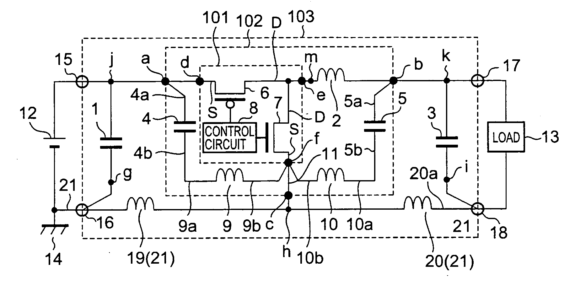
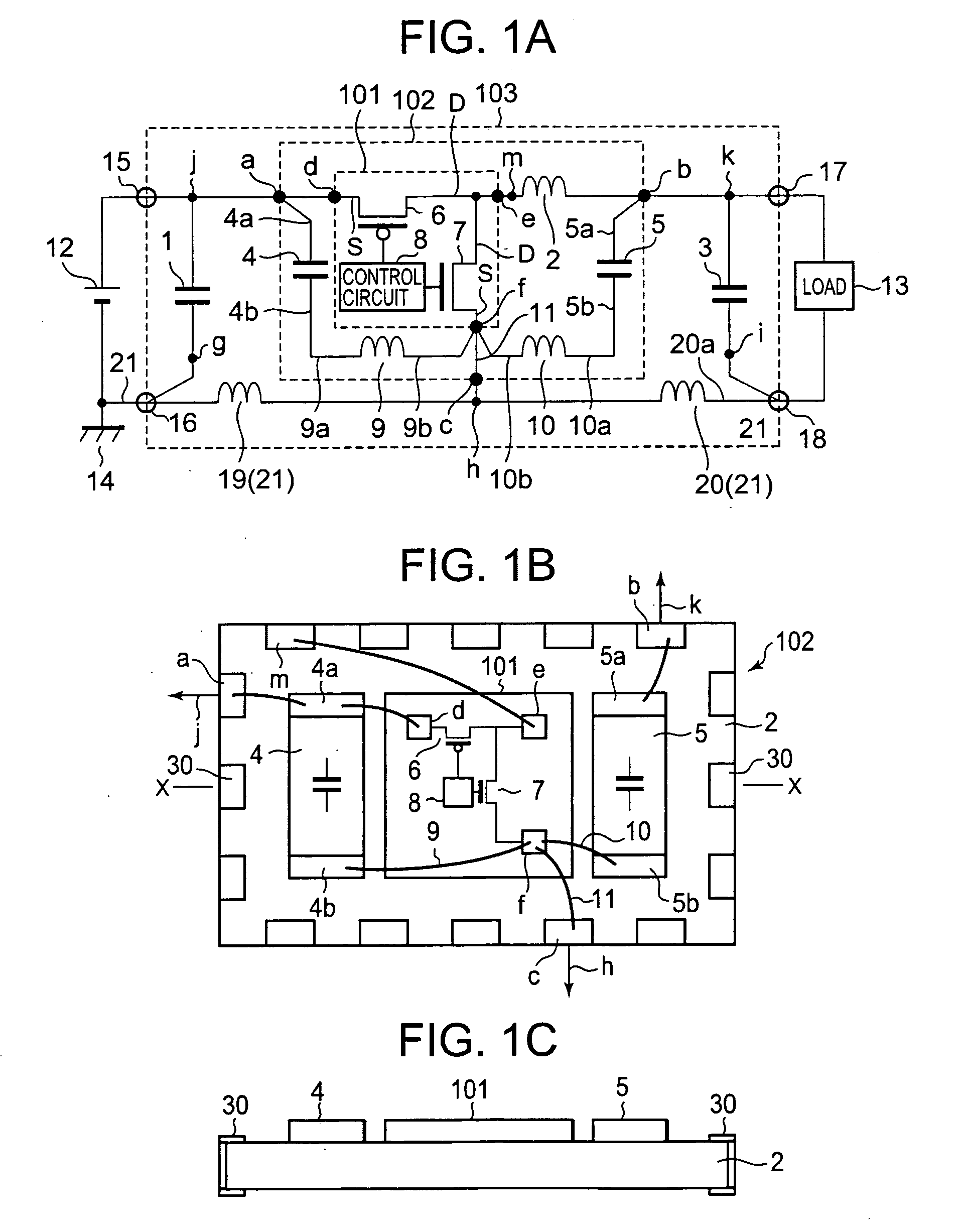
[0050]FIG. 1A is a circuit diagram of important parts of a micro-power source device according to a first embodiment of the invention. FIG. 1B is a plan view of important parts of a micro-power source module according to the first embodiment. FIG. 1C is a sectional view taken along line X-X in FIG. 1B. In FIG. 1A, a micro-power source device 103 (POL power source) is composed of an input capacitor 1, a power source IC 101, an inductor 2, an output capacitor 3, a first noise absorption capacitor 4, and a second noise absorption capacitor 5. A high-potential-side input terminal 15 of the micro-power source device 103, which is connected to a high-potential-side interconnection of an external power source 12, is connected to one terminal j of the input capacitor 1. A ground-side input terminal 16 of the micro-power source device 103, which is connected to a ground 14 of the power source 12, is connected to the other terminal g of the input capacitor 1. The one terminal j of the input c...

embodiment 2

[0055]FIG. 6A is a circuit diagram of important parts of a micro-power source device according to a second embodiment of the invention. FIG. 6B is a plan view of important parts of a micro-power source module according to the second embodiment. FIG. 6C is a sectional view taken along line X-X in FIG. 6B. FIG. 6D is a sectional view of important parts of an integrated capacitor. FIG. 7 is a detailed plan view of an inductor used in the micro-power source module of FIG. 6B. The micro-power source device 108 of FIGS. 6A-6D is different from the micro-power source device 103 of FIGS. 1A-1C in the following points. First, an integrated capacitor 23 as a noise absorption capacitor having a small capacitance on the order of picofarads is formed on the same semiconductor substrate 40 as a power source IC 106 is formed. Second, a divided inductor 22, which is divided at a dividing point r, is used and an intermediate tap q which is connected to the dividing point r is connected to one termin...

embodiment 3

[0061]FIG. 10A is a circuit diagram of important parts of a micro-power source device according to a third embodiment of the invention. FIG. 10B is a plan view of important parts of a micro-power source module according to the third embodiment. FIG. 10C is a sectional view taken along line X-X in FIG. 10B. In this embodiment, a micro-power source module 110 solely constitutes a micro-power source device 111. The micro-power source device 111 according to this embodiment is similar in configuration to the micro-power source device 103 of FIGS. 1A-1C and is different from the latter in that the noise absorption capacitors 4 and 5 are not used and the input capacitor 1 and the output capacitor 3 are mounted on an inductor 27 adjacent to the power source IC 101. In FIGS. 10A-10C, reference numeral 31 denotes a fourth line that connects a terminal 1b of the input capacitor 1 to an input / output terminal 26 (corresponds to the terminal c in FIGS. 1A-1C). Reference numeral 32 denotes a fift...


PUM


Abstract

A power source IC and noise absorption capacitors (decoupling capacitors) are formed on an inductor in such a manner that the noise absorption capacitors are provided on the input side and the output side, respectively. A micro-power source module can'thus be provided which is small in occupied area and height and can reduce conduction noise due to ground lines.

Description

BACKGROUND OF THE INVENTION[0001]1. Field of the Invention[0002]The present invention relates to a micro-power source module, which is part of a micro-power source device used in portable devices, personal computers, etc.[0003]2. Description of the Related Art[0004]Multiple low-voltage supply power sources specific to an LSI (large scale integrated circuit) are mounted on a printed circuit board called a high-speed board in current electronic apparatus. It is desired that the space (area and height) occupied by the low-voltage supply power sources mounted on such a printed circuit board be made as small as possible. The low-voltage supply power sources (power source devices) specific to an LSI are called POL (point of load) power sources. Each of them is composed of discrete components such as a power source IC, an inductor, and capacitors and supplies power to the LSI as a load. The POL power sources are disposed close to the LSI and mounted on the same printed circuit board, as is...

Claims


Application Information

Patent Timeline
Patent Type & Authority Applications(United States)
IPC IPC(8): H03H7/00
CPCH01F17/0033H01F21/12H01L2924/30107H01L2924/12041H01L2224/4917H01L2224/49113H01L2224/48227H01L2224/4813H01L2224/48091H03H1/00H01L2224/48195H01L2924/13091H01L24/49H01L2924/00014H01L2924/00H01L24/48H01L2924/14H01L2224/45099
Inventor NISHIJIMA, KENICHI
Owner FUJI ELECTRIC CO LTD
Why Eureka
Try Eureka