Method of producing electronic apparatus

a technology of electronic equipment and production method, which is applied in the direction of conveyors, manufacturing tools, instruments, etc., can solve the problems of increasing labor expenses concomitantly, affecting the operation time of each step, and the tab method is significant, so as to improve communication characteristics, improve production efficiency, and improve production efficiency.

Inactive Publication Date: 2009-03-05
HITACHI CHEM CO LTD
View PDF11 Cites 12 Cited by
  • Summary
  • Abstract
  • Description
  • Claims
  • Application Information

AI Technical Summary

Benefits of technology

[0012]In light of the above, the object of the present invention is to provide a production method for producing an electronic device at low cost and with superior productivity where the device has satisfactory communication properties.
[0024]The production method for an electronic device according to the present invention finishes the following effects. As a plurality of the IC chips having an external electrode formed respectively on each of the surfaces of an opposing pair are held individually by a plurality of hands each capable of holding one IC chip which hands are arranged around the perimeter of a disc-like conveyor, and by the rotation of this disc-like conveyer a maximum number of the IC chips corresponding to the number of these hands are simultaneously conveyed, then even if the IC chips are each arranged on an antenna substrate and bridging plate superior productivity can be realized and improved communications characteristics are obtained. Further, the available operating time in the production of each inlet is reduced to one second or below one second, and as the IC chips and antenna substrate are connected with the bridging plate via an anisotropic conductive adhesive layers cheaper materials can be used for the base substrate and antenna circuit thereby enabling a more economical inlet to be realized.

Problems solved by technology

In these processes, it is extremely troublesome to make the operating time for each step occur in one second or to reduce this below one second.
This is a substantial problem affecting mass production in this method and thus the TAB method has significant problems.
Further, if the available operating time is long then labor expenses increase concomitantly, mitigating against lower-cost production.
This makes it very difficult to produce the inlet economically.
This creates problems however as complex production equipment is required which increases equipment investment costs, and it is difficult to perform mass production of the inlets at low cost.
There are problems confronting this method that employs a disc-like conveyor however.

Method used


Image

  • Method of producing electronic apparatus
  • Method of producing electronic apparatus
  • Method of producing electronic apparatus

Examples


embodiment 1

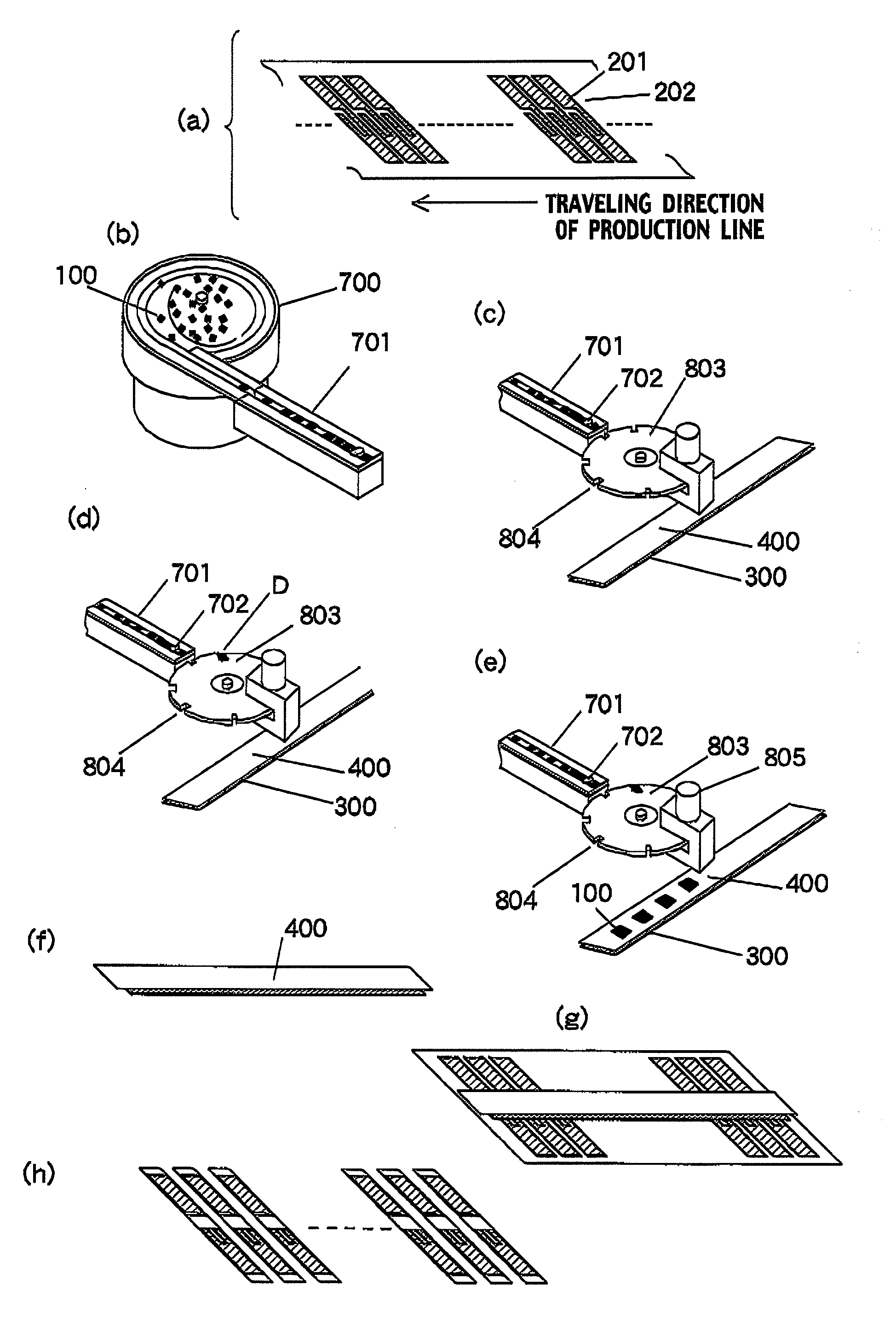
[0064]A first embodiment of the present invention will now be described with reference to FIG. 3.

[0065]As shown in FIG. 3 (a), an etching resist is formed by screen printing on an aluminum foil surface of a tape form substrate produced by adhering aluminum foil of a thickness of 9 μm to a polyethylene terephthalate substrate 202 of a thickness of 50 μm using an adhesive agent. Next, an antenna circuit 201 is formed continuously on the aluminum foil surface using ferric chloride solution as an etching liquid. Here, the antenna thickness for each antenna circuit is 2.5 mm, the thickness of the slit is 0.5 mm, and the antenna circuits are formed at a pitch of 3 mm.

[0066]As shown in FIG. 3b), after approximately 10000 IC chips 100 each having a thickness of 0.15 mm and a length and width both of 0.4 mm and having an external electrode formed respectively on the surfaces of each of the opposing pair of surfaces thereof are supplied to a high frequency parts feeder 700, that high-frequenc...

embodiment 2

[0075]A second embodiment of the present invention will now be described with reference to FIG. 4.

[0076]As shown in FIG. 4 (a), an etching resist is formed by screen printing on an aluminum foil surface of a tape form substrate produced by adhering aluminum foil of a thickness of 9 μm to a polyethylene terephthalate substrate 202 of a thickness of 50 μm using an adhesive agent. Next, an antenna circuit 201 is formed continuously on the aluminum foil surface using ferric chloride solution as an etching liquid. Here, the antenna thickness for each antenna circuit is 2.5 mm, the thickness of the slit is 0.5 mm, and the antenna circuits are formed at a pitch of 3 mm.

[0077]Next, as shown in FIG. 4 (b) an anisotropic conductive adhesive layer is formed in the determined position on an antenna circuit by lamination at a temperature of 80° C. of an anisotropic conductive adhesive film 400 (AC-2052P-45 by Hitachi Chemical Co. Ltd.) having a width of 2.5 mm, and then removal of the separator ...

embodiment 3

[0087]The third embodiment will now be described.

[0088]Up until the step shown in FIG. 4 (f) the same processes are used as those with respect to embodiment 2, involving processing of the antenna substrate, laminating the anisotropic conductive adhesive film on the antenna circuit and forming the anisotropic conductive adhesive layer, arranging the IC chips having the external electrode formed on each of the surfaces of the pair of facing surfaces and then securing each of the IC chips in the determined position on the antenna circuit.

[0089]Next, an anisotropic conductive adhesive film of the same width as the above laminated anisotropic conductive adhesive film is laminated at 80° C. over the tentatively secured IC chips, and the separator film is then removed thus forming an anisotropic conductive adhesive layer.

[0090]Then, a tape form substrate 2 mm wide is prepared, by adhering aluminum foil of a thickness of 9 μm on a polyethylene terephalate substrate 50 μm thick using adhesiv...


PUM

PropertyMeasurementUnit
timeaaaaaaaaaa
temperaturesaaaaaaaaaa
thicknessaaaaaaaaaa

Abstract

To provide a method of producing an electronic apparatus that is inexpensive, contributes to high productivity, and can achieve good communication characteristics. A method of producing an electronic apparatus composed of an IC chip (100) having an external electrode formed on each of a set of opposing surfaces of the IC chip; an antenna circuit (201) having a slit formed in it; and a short circuit plate (300) for electrically connecting the IC chip (100) and the antenna circuit (201). In the method, a disc-like conveyor (703) has hands (704) on its outer periphery, and each hand (704) is capable of holding a single IC chip (100). The hands (704) hold IC chips (100) individually, and the IC chips (100) are conveyed by rotation of the disc-like conveyor (703). As a result, a plurality of IC chips (100) whose maximum number is equal to the number of the hands (704) can be simultaneously conveyed.

Description

TECHNICAL FIELD[0001]The present invention relates to a method for producing economically and with improved productivity, an electronic device having good communications characteristics, used for a noncontact type individual identification device mounted with an IC chip.BACKGROUND ART[0002]In recent years non-contact type individual identification systems that employ RFID (Radio Frequency Identification) tags have been focused on for use in systems for managing the entire lifecycle of a product, including all commercial aspects of production of a product, it's distribution and sales. Radio wave type RFID tags that use 2.45 GHz microwaves are noted for the structure that includes an external antenna attached to an IC element that enables communication to be performed over several meters. Presently, construction is ongoing of systems that operate for distribution of mass-produced products as well as their product management and production history management.[0003]Current examples of r...

Claims


Application Information

Patent Timeline
Patent Type & Authority Applications(United States)
IPC IPC(8): H01L21/50
CPCG06K19/07749G06K19/0775G06K19/07786H01L21/67132H01L23/49855H01L24/33H01L24/75H01L24/83H01L24/97H01L2223/6677H01L2224/2518H01L2224/83102H01L2224/83192H01L2224/83856H01L2224/92125H01L2224/97H01L2924/01005H01L2924/01013H01L2924/01015H01L2924/01027H01L2924/01029H01L2924/01033H01L2924/01047H01L2924/0105H01L2924/01074H01L2924/01078H01L2924/01079H01L2924/01082H01L2924/0781H01L2924/14H01L2924/19041H01L2924/19043H01L2924/3011H01L2924/01006H01L2924/01019H01L2924/014H01L2924/0132H01L2224/16225H01L2224/29111H01L2224/32225H01L2224/73204H01L2224/29299H01L2224/2929H01L2924/00013H01L2224/16227H01L2224/81191H01L2924/07811Y10T29/5313Y10T29/53174Y10T29/53178H01L2224/83H01L2924/00H01L2924/00015H01L2924/00014H01L2224/29099H01L2224/29199G06K19/07
Inventor TANAKA, KOUSUKEISHIZAKA, HIRONORITASAKI, KOUJISHIBUTANI, MASAHITOSHINZAWA, MASAHISAKONNO, SHIGEHIROIWATA, KATSUYA
Owner HITACHI CHEM CO LTD
Why Eureka
Try Eureka