Method and structure for hydrogenation of silicon substrates with shaped covers

a silicon substrate and hydrogenation technology, applied in the field of solar energy techniques, can solve the problems of increasing the cost of silicon substrates, and increasing the cost of silicon substrates, and achieve the effect of less cost and easy handling

Inactive Publication Date: 2009-03-12
SILICON CHINA HK
View PDF9 Cites 38 Cited by
  • Summary
  • Abstract
  • Description
  • Claims
  • Application Information

AI Technical Summary

Benefits of technology

[0014]Many benefits are achieved by way of the present invention over conventional techniques. For example, the present technique provides an easy way to use process that relies upon conventional technology such as silicon materials, although other materials can also be used. Additionally, the method provides a process that is compatible with conventional process technology without substantial modifications to conventional equipment and processes. Preferably, the invention provides for an improved solar cell, which is less costly and easy to handle. Such solar cell uses a hydrogen co-implant to form a thin layer of photovoltaic material. Since the layers are very thin, multiple layers of photovoltaic regions can be formed from a single conventional single crystal silicon or other like material wafer. In a preferred embodiment, the present thin layer removed by hydrogen implant and thermal treatment can be provided on a low grade substrate material, which will serve as a support member. Depending upon the embodiment, one or more of these benefits may be achieved. These and other benefits will be described in more detail throughout the present specification and more particularly below.

Problems solved by technology

Greenhouse gases are evolving a rapid rates, leading to global warming.
As the population of the world increases rapidly to over six billion people, there has been an equally large consumption of energy resources, which leads to additional greenhouse gases.
As merely an example, further increases in oil consumption have been projected.
Oil is becoming increasingly scarce.
Unfortunately, solar cells still have limitations although solar panels have been used successfully for certain applications.
As an example, solar cells are often costly.
Solar cells are often composed of silicon bearing wafer materials, which are difficult to manufacture efficiently on a large scale.
Availability of solar cells made of silicon is also somewhat scarce with limited silicon manufacturing capacities.

Method used


Image

  • Method and structure for hydrogenation of silicon substrates with shaped covers
  • Method and structure for hydrogenation of silicon substrates with shaped covers
  • Method and structure for hydrogenation of silicon substrates with shaped covers

Examples


embodiment

General Method Embodiment

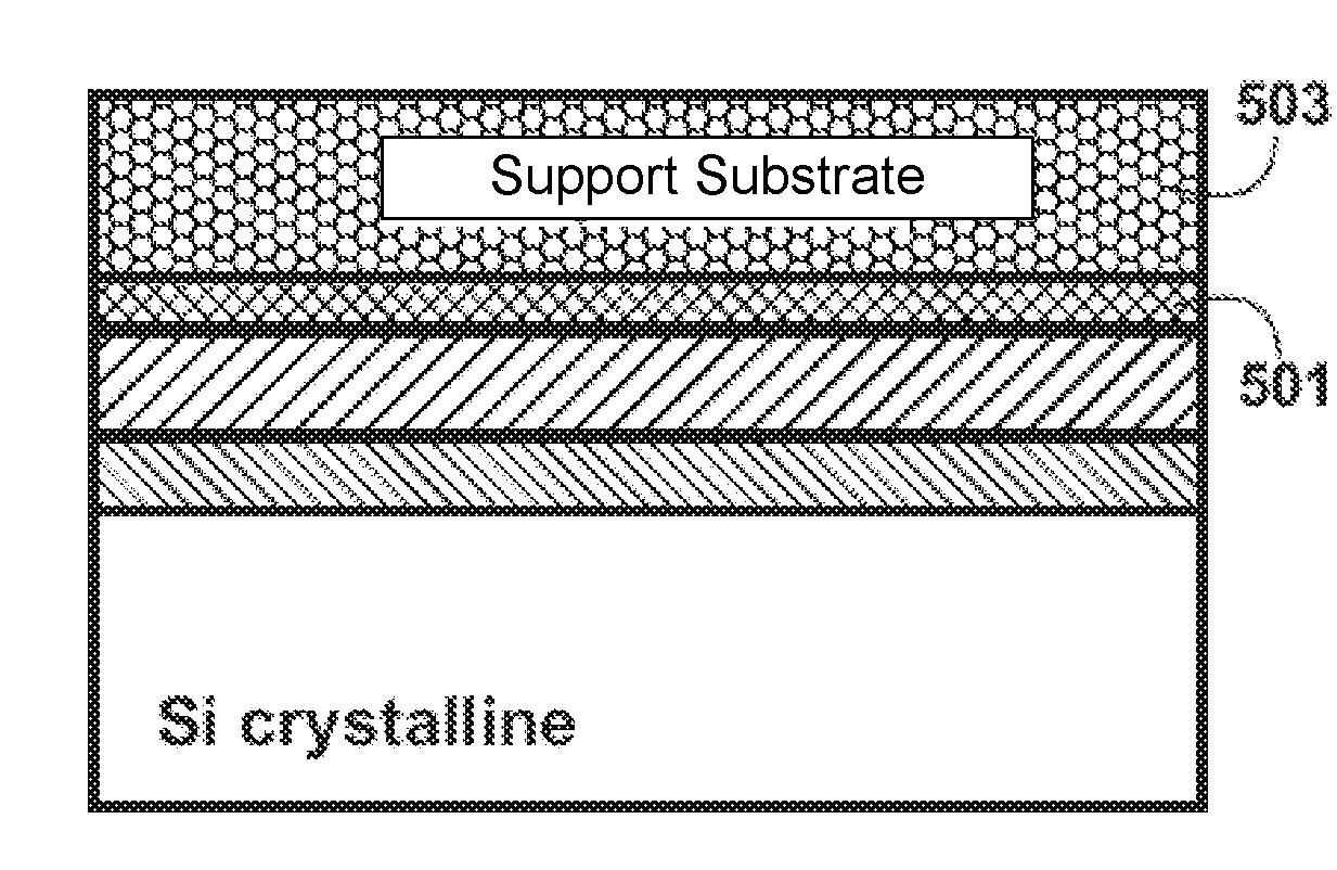
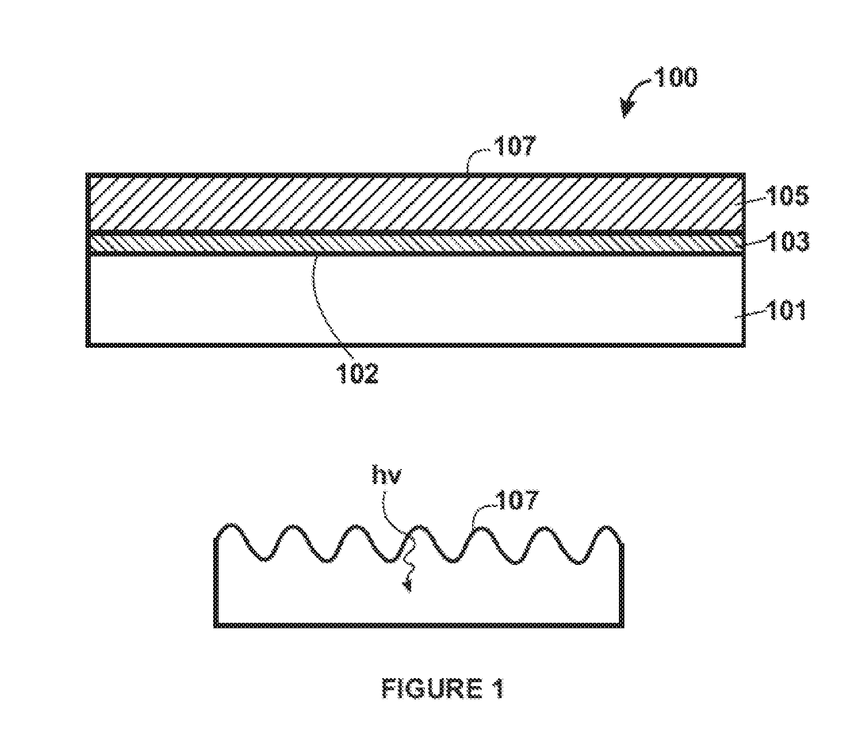
[0032]In a specific embodiment, the present invention provides a method for fabricating a photovoltaic device that can be outlined as follows:[0033]1. Provide a semiconductor substrate, e.g., single crystal silicon, silicon germanium, Group II / VI, Group III / V;[0034]2. Form a crystalline material characterized by a plurality of worm hole structures therein overlying the semiconductor substrate[0035]3. Subject the crystalline material to a hydrogen plasma species to occupy at least one or more of the worm hole structures therein of the crystalline material within a vicinity of an interface between the thickness of material and a remaining portion of the semiconductor substrate;[0036]4. Provide a glue layer overlying a surface region of the crystalline material;[0037]5. Join the surface region of the crystalline material via the glue layer to a support substrate;[0038]6. Delaminate a portion of the crystalline material from the semiconductor substrate;[0039]7. ...


PUM

PropertyMeasurementUnit
roughnessaaaaaaaaaa
surface roughnessaaaaaaaaaa

Abstract

Method and structure for hydrogenation of silicon substrates with shaped covers. According to an embodiment, the present invention provides a method for fabricating a photovoltaic material. The method includes providing a semiconductor substrate. The method also includes forming a crystalline material characterized by a plurality of worm hole structures therein overlying the semiconductor substrate. The worm hole structures are characterized by a density distribution from a surface region of the crystalline material to a defined depth within a z-direction of the surface region to form a thickness of material to be detached. The method further includes providing a glue layer overlying a surface region of the crystalline material. The method includes joining the surface region of the crystalline material via the glue layer to a support substrate.

Description

CROSS-REFERENCE TO RELATED APPLICATION[0001]This application claims priority to U.S. Provisional Application No. 60 / 971,528 titled “Method and Structure for Hydrogenation of Silicon Substrates with Shaped Covers” filed Sep. 11, 2007, which is incorporated by reference herein.BACKGROUND OF THE INVENTION[0002]The present invention relates generally to solar energy techniques. In particular, the present invention provides a method and resulting device fabricated from a hydrogen separation process using a crystalline porous material suitable for photovoltaic applications. More particularly, the present invention provides a method and resulting device for manufacturing the photovoltaic regions within the single crystal porous material on a substrate member, and the performance of the photovoltaic region is enhanced by a shaped cover. For example, the shape cover includes angled facets for light trapping. Merely by way of example, the invention has been applied to solar panels, commonly t...

Claims


Application Information

Patent Timeline
Patent Type & Authority Applications(United States)
IPC IPC(8): H01L31/00
CPCH01L31/0236H01L31/18Y10T156/11Y02E10/50H01L31/1892
Inventor CHAN, YICK CHUENHO, PUI YEECHEUNG, NATHAN W.CHAN, CHUNG
Owner SILICON CHINA HK
Why Eureka
Try Eureka