Wireless IC device and wireless IC device composite component

Active Publication Date: 2009-03-12
MURATA MFG CO LTD
View PDF14 Cites 153 Cited by
  • Summary
  • Abstract
  • Description
  • Claims
  • Application Information

AI Technical Summary

Benefits of technology

[0013]Furthermore, since the inductance element defining the feed circuit is provided in the high-permeability magnetic body, it is possible to increase the Q value of the inductance

Problems solved by technology

However, it is very difficult to accurately mount the wireless IC chip 301 on the large support film 305, and there is a problem in that the resonant f

Method used


Image

  • Wireless IC device and wireless IC device composite component
  • Wireless IC device and wireless IC device composite component
  • Wireless IC device and wireless IC device composite component

Examples


first preferred embodiment

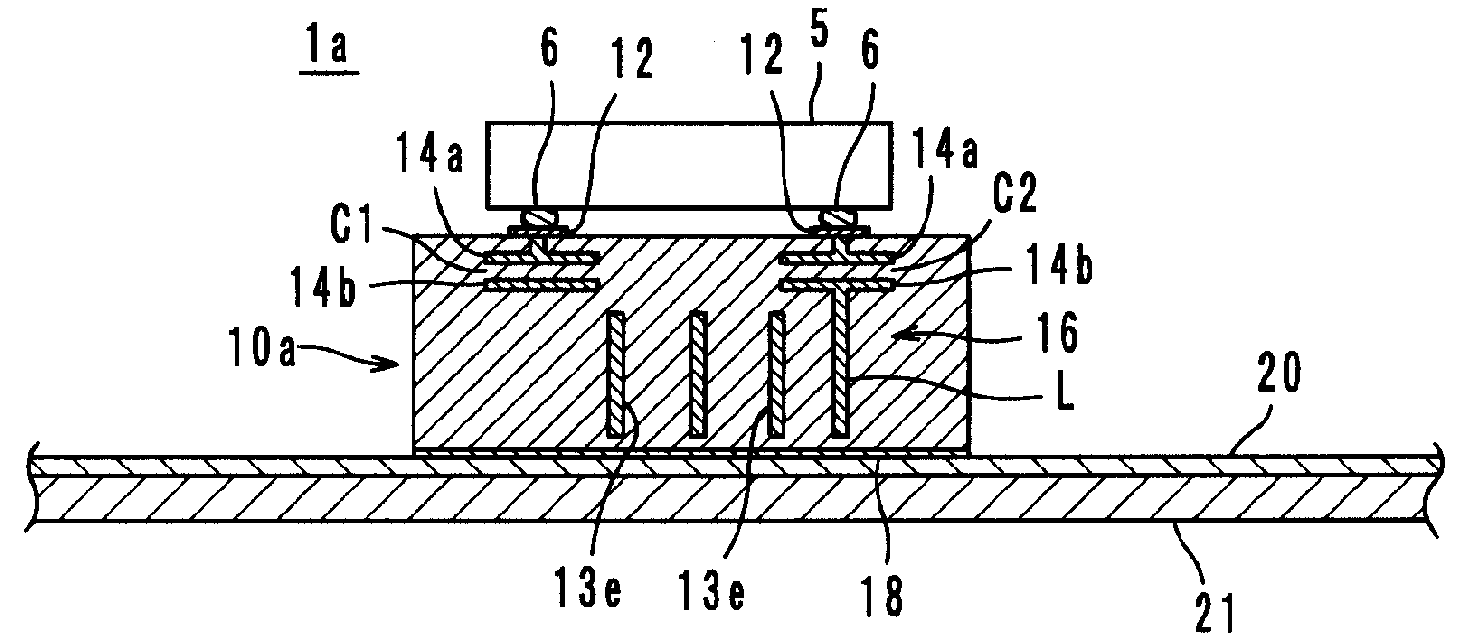
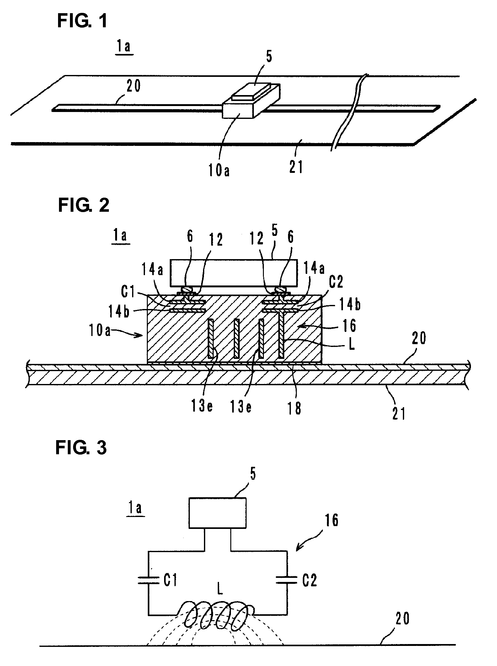
[0082]A wireless IC device 1a according to a first preferred embodiment of the present invention includes a monopole type radiation plate. As shown in FIGS. 1 and 2, the wireless IC device 1a includes a wireless IC chip 5, a feed circuit board 10a having the wireless IC chip 5 mounted on the top surface thereof, and a radiation plate 20 to which the feed circuit board 10a is adhered. The wireless IC chip 5 may preferably include clock circuits, logic circuits, and memory circuits and has necessary information stored therein. The wireless IC chip 5 is directly DC-connected to a feed circuit 16 included in the feed circuit board 10a.

[0083]The feed circuit board 10a is a ceramic multilayer board made of a magnetic ceramic material having a high permeability. The feed circuit 16 is a circuit arranged to supply a transmission signal having a predetermined frequency to the radiation plate 20 and / or a circuit arranged to select a reception signal having a predetermined frequency from sign...

second preferred embodiment

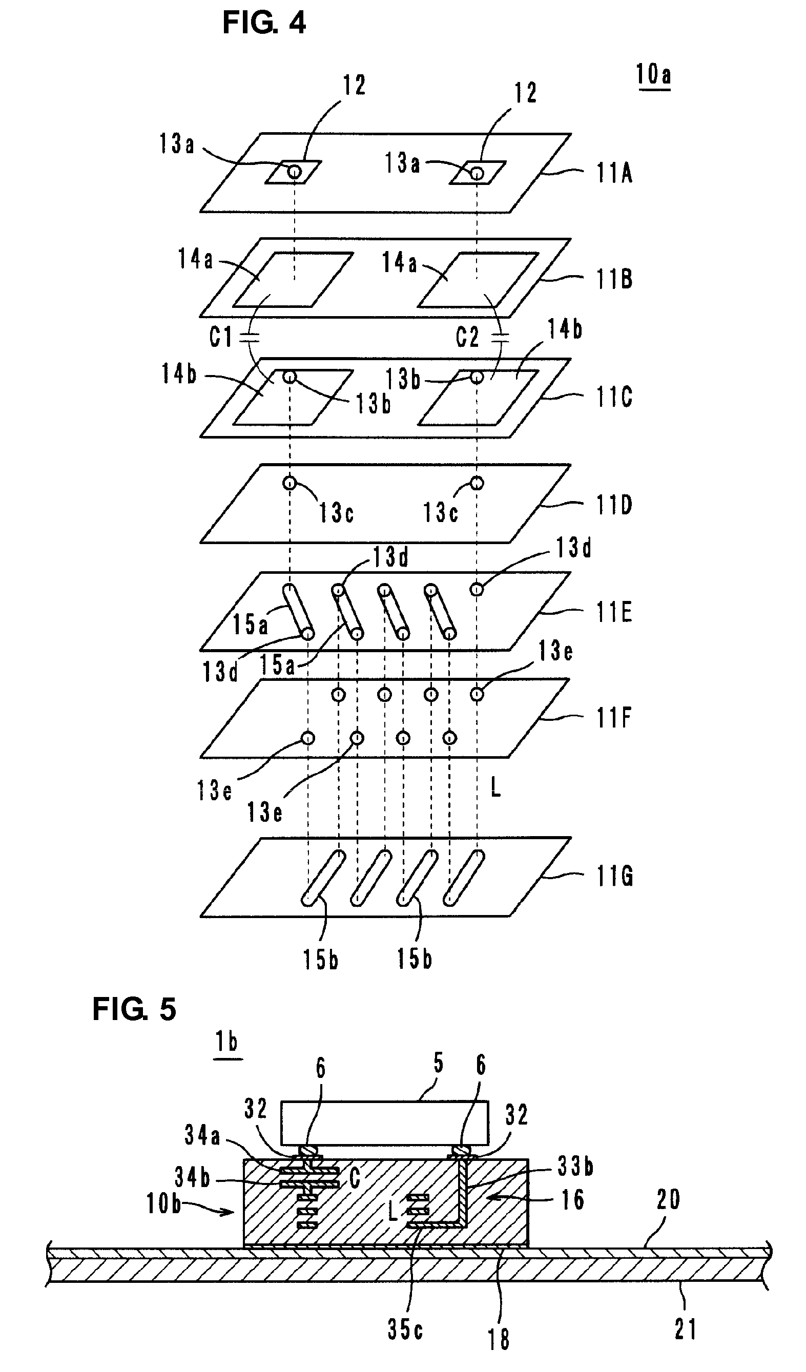
[0096]A wireless IC device 1b according to a second referred embodiment of the present invention is provided with a monopole type radiation plate, as shown in FIG. 5. The wireless IC device 1b includes the feed circuit 16 that is included in a feed circuit board 10b and that is defined by an LC series resonant circuit including an inductance element L and a capacitance element C. As shown in FIG. 6, the winding axis of the coil electrode pattern defining the inductance element L is perpendicular or substantially perpendicular to the radiation plate 20, and the feed circuit 16 is primarily magnetically coupled to the radiation plate 20.

[0097]Specifically, as shown in FIG. 7, the feed circuit board 10b is manufactured by layering, attaching by pressure, and firing ceramic sheets 31A to 31F defined by high-permeability magnetic bodies. The feed circuit board 10b includes the sheet 31A on which connection electrodes 32 and via-hole conductors 33a are provided, the sheet 31B on which a c...

third preferred embodiment

[0102]In a wireless IC device 1d according to a third preferred embodiment of the present invention, as shown in FIG. 9, the wireless IC chip 5 is mounted on a first main surface 110 of a feed circuit board 10d defined by a high-permeability magnetic body and a radiation plate (not shown) is provided on a second main surface 120 of the feed circuit board 10d. FIG. 9 shows a wireless IC device composite component including the wireless IC chip 5 and the feed circuit board 10d.

[0103]The feed circuit board 10d has a multilayer structure which includes capacitance electrodes defining the capacitance elements C1 and C2 and the inductance elements L1 and L2, and in which high-permeability magnetic layers 100 preferably made of a high-permeability magnetic ceramic material are layered, as shown in FIG. 10.

[0104]In the wireless IC device 1d, as shown as an equivalent circuit in FIG. 11, the feed circuit 16 includes the inductance elements L1 and L2 magnetically coupled to each other (denot...


PUM


Abstract

A wireless IC device includes a wireless IC chip, a feed circuit board having the wireless IC chip mounted thereon and including a feed circuit including inductance elements, and a radiation plate electromagnetically coupled to the inductance elements in the feed circuit. A high-permeability magnetic body made of a high-permeability magnetic material is provided in the feed circuit board and a portion of the inductance elements is provided in the high-permeability magnetic body.

Description

BACKGROUND OF THE INVENTION[0001]1. Field of the Invention[0002]The present invention relates to wireless integrated circuit (IC) devices. More particularly, the present invention relates to a wireless IC device used in a radio frequency identification (RFID) system and a wireless IC device composite component used in the wireless IC device.[0003]2. Description of the Related Art[0004]Recently, RFID systems have been developed as management systems of articles. In a typical RFID system, a reader-writer that generates an induction field communicates with a wireless tag (hereinafter referred to as a wireless IC device) that is attached to an article, that stores certain information, and that transmits the information in a non-contact manner.[0005]Wireless IC devices used in the RFID systems are disclosed in, for example, U.S. Pat. No. 6,406,990 and U.S. Pat. No. 6,664,645.[0006]Specifically, a wireless IC device shown in FIG. 32 is disclosed, in which an air-core type antenna pattern ...

Claims


Application Information

Patent Timeline
IPC IPC(8): G06K19/077
CPCG06K19/07749H01L2224/16225G06K19/07779G06K19/07783G06K19/07784H01F17/0006H01F38/14H01L23/49855H01L2924/09701H01L2924/3011H01Q1/2208H01Q1/2283H01Q1/242H01Q1/50H01Q7/00H01Q23/00H01Q25/02G06K19/07756
Inventor KATO, NOBORUDOKAI, YUYAISHINO, SATOSHI
Owner MURATA MFG CO LTD
Why Eureka
Try Eureka