Semiconductor device and fabrication method for the same

a technology of semiconductors and semiconductors, applied in the direction of semiconductor devices, electrical equipment, transistors, etc., can solve the disadvantages of complex fabrication process, and achieve the effect of simplifying the method of fabrication

Inactive Publication Date: 2009-03-12
PANASONIC CORP
View PDF4 Cites 11 Cited by
  • Summary
  • Abstract
  • Description
  • Claims
  • Application Information

AI Technical Summary

Benefits of technology

[0020]An object of the present invention is providing a simpler method for fabricating a semiconductor device in which different types of stress are produced for MIS transistors different in conductivity type.

Problems solved by technology

However, in the conventional fabrication method for a semiconductor device described above, in which different types of stress must be produced in the channel regions of the n-type transistor region A and the p-type transistor region B, the fabrication process is disadvantageously complicated.

Method used


Image

  • Semiconductor device and fabrication method for the same
  • Semiconductor device and fabrication method for the same
  • Semiconductor device and fabrication method for the same

Examples


embodiment 1

Alteration to Embodiment 1

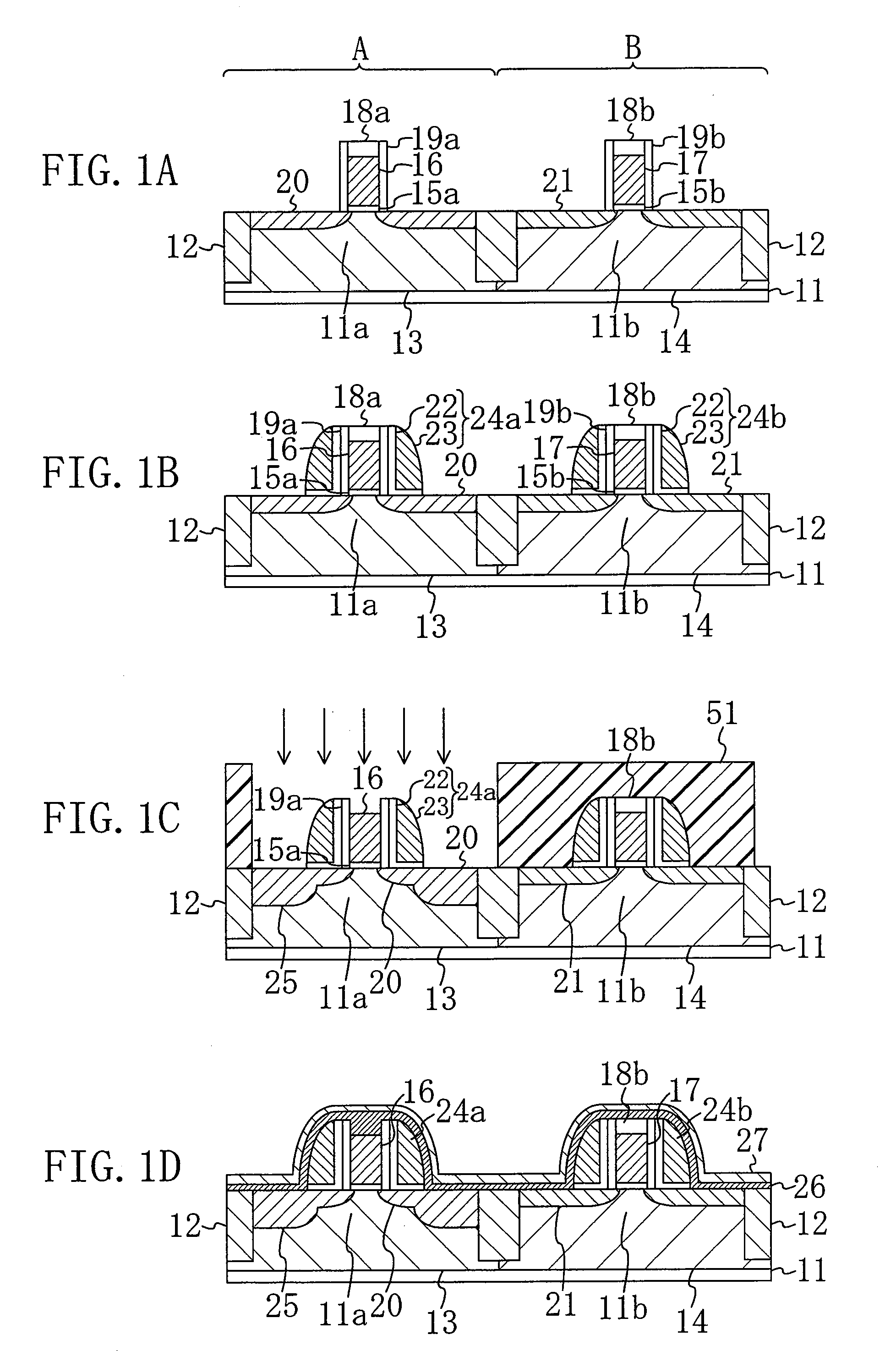
[0071]A fabrication method for a semiconductor device of an alteration to Embodiment 1 of the present invention will be described with reference to FIGS. 4A to 4C, in which the same components as those in FIGS. 3A to 3C are denoted by the same reference numerals, and description thereof is omitted here.

[0072]FIG. 4A shows a process step to be executed after the process step shown in FIG. 3B in the fabrication method for a semiconductor device of Embodiment 1, as an alternation to Embodiment 1.

[0073]Specifically, the silicon nitride film 23 located outside, among the silicon oxide film 22 and the silicon nitride film 23 constituting each of the sidewalls 24a and 24b on the n-type gate electrode 16 and the p-type gate electrode 17, is selectively removed with hot phosphoric acid, for example.

[0074]As shown in FIG. 4B, as in Embodiment 1, a metal layer made of Ni, Co or Pt, for example, is deposited on the resultant semiconductor substrate 11 by sputtering and...

embodiment 2

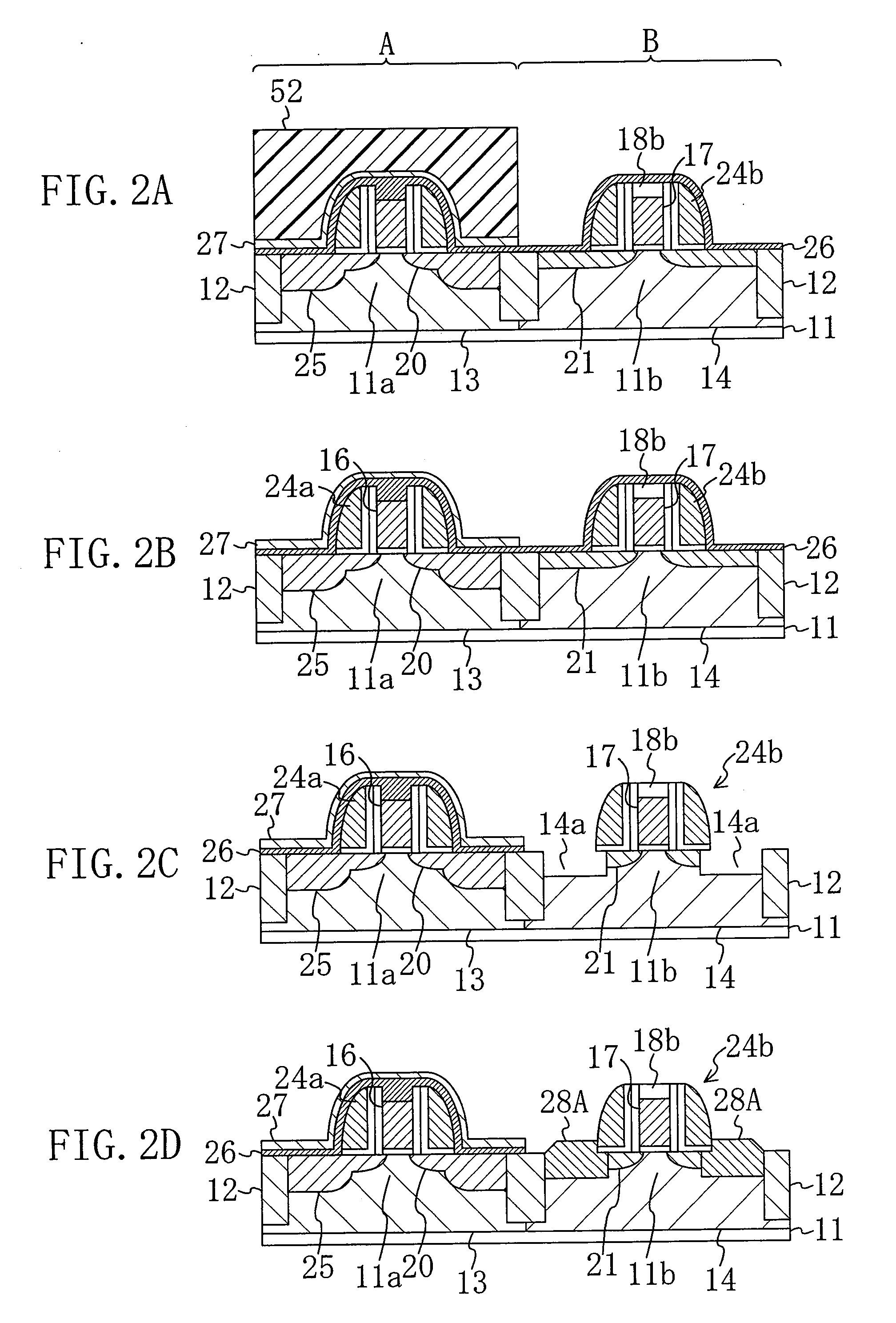
[0079]A fabrication method for a semiconductor device of Embodiment 2 of the present invention will be described with reference to the relevant drawings.

[0080]FIGS. 5A to 5D, 6A to 6D and 7A to 7C are cross-sectional views sequentially illustrating process steps of a fabrication method for a semiconductor device of Embodiment 2 of the present invention.

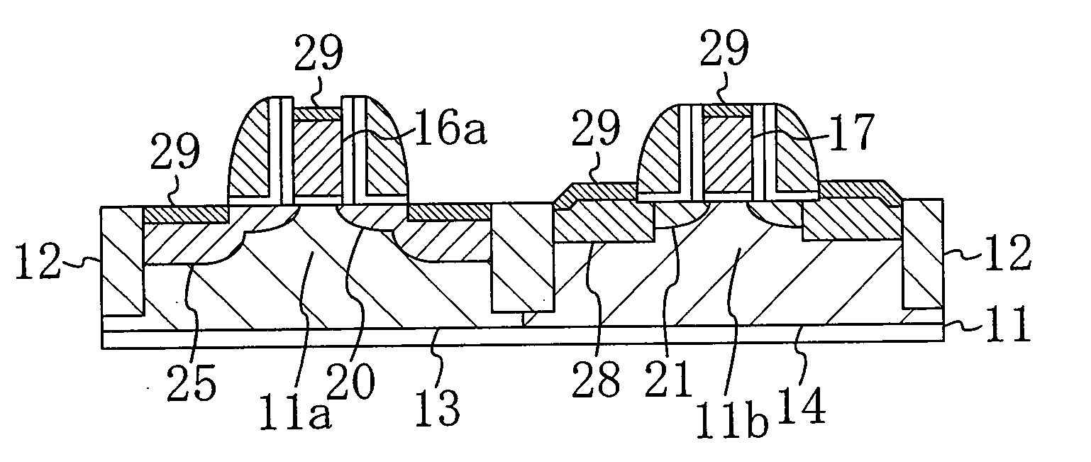
[0081]First, as shown in FIG. 5A, the principal surface of a semiconductor substrate 11 made of silicon (Si), which has (100) plane as its principal surface, is partitioned into an n-type transistor region A and a p-type transistor region B with an isolation region 12. An active region 11a is therefore formed as a portion of the semiconductor substrate 11 surrounded with the isolation region 12 in the n-type transistor region A, and an active region 11b is formed as a portion of the semiconductor substrate 11 surrounded with the isolation region 12 in the p-type transistor region B. A p-type well 13 is then formed in the n-type transi...


PUM


Abstract

The semiconductor device includes: a first MIS transistor formed on a first region of a first conductivity type in a semiconductor substrate; and a second MIS transistor formed on a second region of a second conductivity type in the semiconductor substrate. The first MIS transistor has a first gate insulating film and a first gate electrode formed on the first region, first sidewalls formed on the side faces of the first gate electrode, and first source/drain regions made of silicon formed in portions of the first region. The second MIS transistor has a second gate insulating film and a second gate electrode formed on the second region, second sidewalls formed on the side faces of the second gate electrode, and second source/drain regions including silicon germanium formed in portions of the second region. The second sidewalls are smaller in height than the first sidewalls.

Description

CROSS-REFERENCE TO RELATED APPLICATIONS[0001]This application claims priority under 35 U.S.C. §119 on Patent Application No. 2007-232556 filed in Japan on Sep. 7, 2007, the entire contents of which are hereby incorporated by reference.BACKGROUND OF THE INVENTION[0002]The present invention relates to a semiconductor device and a fabrication method for the same, and more particularly to a semiconductor device in which stress strain is imparted to the channel region of a metal-insulator semiconductor (MIS) transistor and a fabrication method for such a semiconductor device.[0003]In recent years, along with implementation of semiconductor integrated circuit devices with higher integration, higher performance and higher speed, there has been proposed a technology of improving the carrier mobility by imparting stress strain to the semiconductor substrate. For example, the mobility of electrons improves by imparting tensile stress strain to an n-type MIS transistor formed on the principal ...

Claims


Application Information

Patent Timeline
Patent Type & Authority Applications(United States)
IPC IPC(8): H01L27/092H01L21/8238
CPCH01L21/823807H01L21/823814H01L29/7843H01L21/823864H01L21/823842
Inventor FUJIMOTO, HIROMASA
Owner PANASONIC CORP
Why Eureka
Try Eureka