Image Sensor and Manufacturing Method Thereof

Inactive Publication Date: 2009-03-12
MARVELL ASIA PTE LTD
View PDF13 Cites 125 Cited by
  • Summary
  • Abstract
  • Description
  • Claims
  • Application Information

AI Technical Summary

Benefits of technology

[0009]Embodiments of the present invention provide an image sensor that can improve bonding force of a bonding surface during a wafer-to-wafer bonding op

Problems solved by technology

As the size of a photodiode reduces more and more for the purpose of increasing the number of pixels without an increase in a chip size, the area of a light receiving portion reduces, so that an image quality reduces.
Also, according to a related art, a dark defect may be generated in a photod

Method used


Image

  • Image Sensor and Manufacturing Method Thereof
  • Image Sensor and Manufacturing Method Thereof
  • Image Sensor and Manufacturing Method Thereof

Examples


Example

[0015]Embodiments of an image sensor and a manufacturing method thereof according to an embodiment will be described in detail with reference to the accompanying drawings.

[0016]FIG. 13 is a cross-sectional view of an image sensor according to an embodiment.

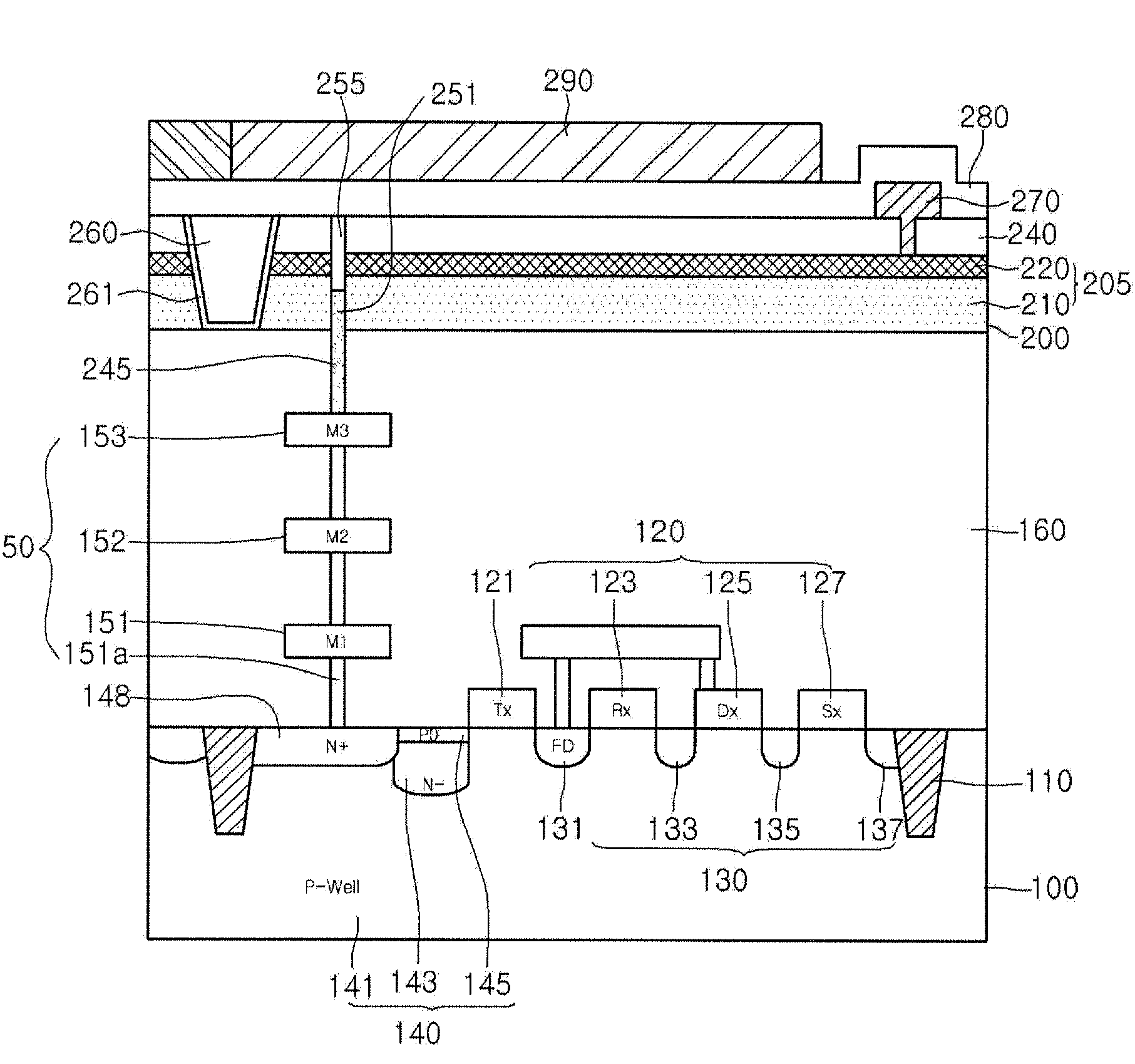
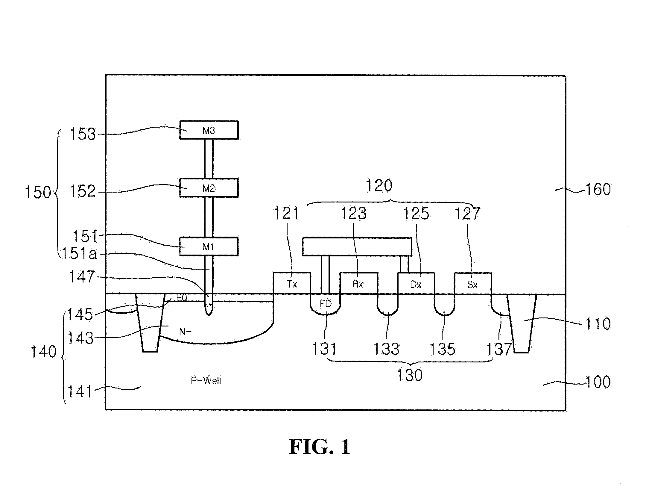
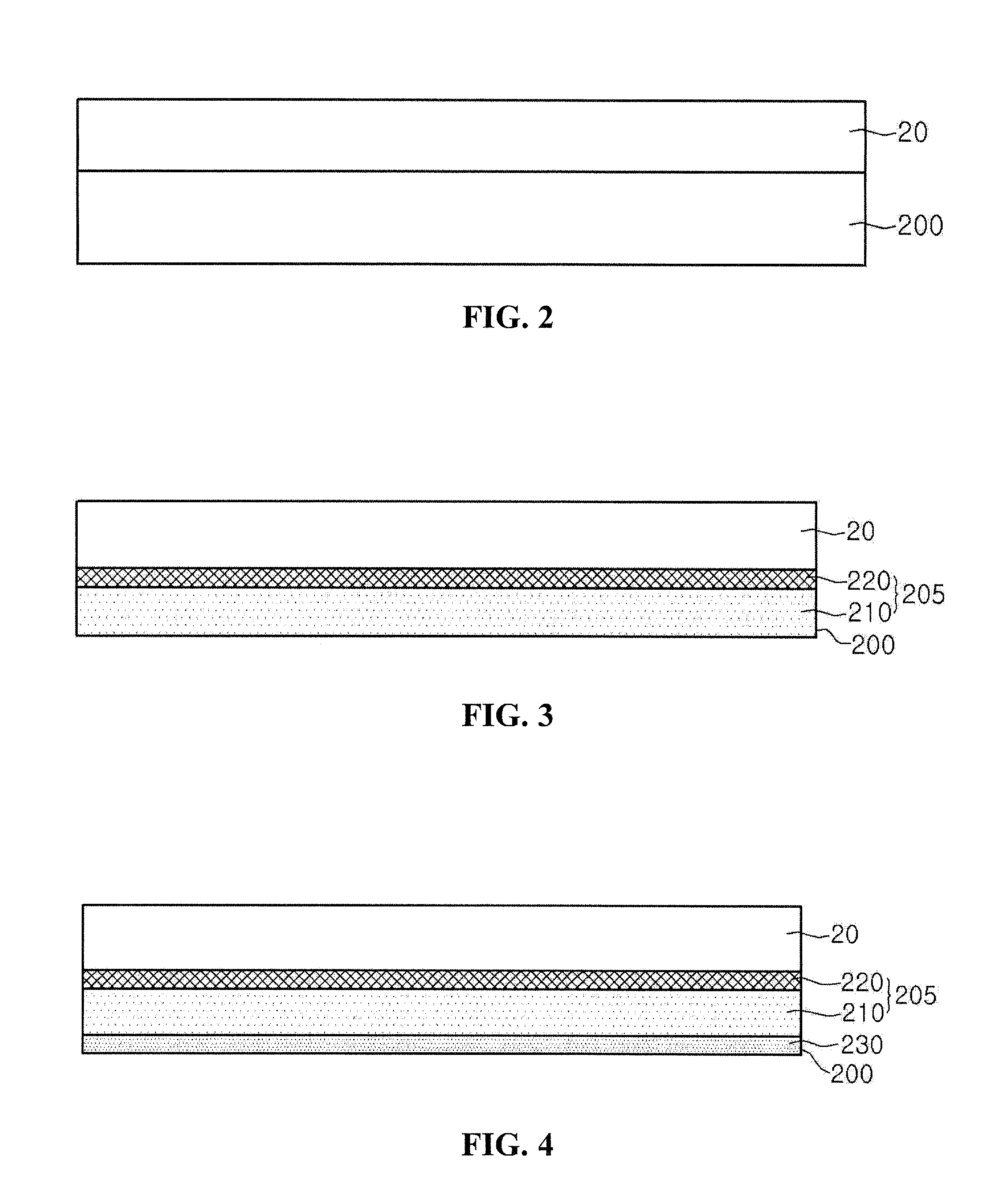
[0017]Referring to FIG. 13, an image sensor can include: a first substrate 100 including a readout circuitry 120; an interlayer dielectric 160 on the first substrate, the interlayer dielectric including a lower line 150 therein; a crystalline semiconductor layer 200 on the interlayer dielectric 160; a photodiode 205 in the crystalline semiconductor layer 200, the photodiode being formed of a stacked first impurity region 210 and second impurity region 220; a via hole 245 passing through the crystalline semiconductor layer 200 and the interlayer dielectric 160 to expose the lower line 150; a plug 251 formed inside the first via hole 245 to connect with only the lower line 150 and the first impurity region 210; and a device isolatio...


PUM


Abstract

Provided is an image sensor. The image sensor can include a readout circuitry on a first substrate. An interlayer dielectric is formed on the first substrate, and comprises a lower line therein. A crystalline semiconductor layer is bonded to the interlayer dielectric. A photodiode can be formed in the crystalline semiconductor layer, and comprises a first impurity region and a second impurity region. A via hole can be formed passing through the crystalline semiconductor layer and the interlayer dielectric to expose the lower line. A plug is formed inside the first via hole to connect with only the lower line and the first impurity region. A device isolation region can be formed in the crystalline semiconductor layer to separate the photodiode according to unit pixel.

Description

CROSS-REFERENCE TO RELATED APPLICATIONS[0001]The present application claims the benefit under 35 U.S.C. §119 of Korean Patent Application No. 10-2007-0090866, filed Sep. 9, 2007, and Korean Patent Application No. 10-2008-0059721, filed Jun. 24, 2008, which are hereby incorporated by reference in their entirety.BACKGROUND[0002]An image sensor is a semiconductor device for converting an optical image into an electrical signal. The image sensor is roughly classified as a charge coupled device (CCD) image sensor or a complementary metal oxide semiconductor (CMOS) image sensor (CIS).[0003]In an image sensor, a photodiode is formed in a substrate having readout circuitry using ion implantation. As the size of a photodiode reduces more and more for the purpose of increasing the number of pixels without an increase in a chip size, the area of a light receiving portion reduces, so that an image quality reduces.[0004]Also, since a stack height does not reduce as much as the reduction in the a...

Claims


Application Information

Patent Timeline
IPC IPC(8): H01L31/112H01L31/02
CPCH01L27/14603H01L27/14609H01L27/14621H01L27/1463H01L27/14687H01L27/14634H01L27/14636H01L27/14643H01L27/14632
Inventor HWANG, JOON
Owner MARVELL ASIA PTE LTD
Why Eureka
Try Eureka