Metal wiring of a semiconductor device and method of forming the same

a technology of metal wiring and semiconductor devices, applied in semiconductor devices, semiconductor/solid-state device details, electrical apparatus, etc., can solve the problem of excessive removal of conductive material layers, and achieve the effect of improving one or more electrical properties and reducing process difficulty

Inactive Publication Date: 2009-03-12
SK HYNIX INC
View PDF3 Cites 8 Cited by
  • Summary
  • Abstract
  • Description
  • Claims
  • Application Information

AI Technical Summary

Benefits of technology

[0004]According to a metal wiring of a semiconductor substrate and a method of forming the same disclosed herein, the contact plug is formed at lower height than the contact hole, which is formed on the interlayer insulation layer, and then a metal wiring is formed over the contact plug and interlayer insulation layer. The method and apparatus can have one or more advantages, such as completely filling the inside of the contact hole, decreasing process difficulty, ensuring reproducibility, and improving one or more electrical properties.

Problems solved by technology

Additionally, H2O2 contained in slurry that is used in the polishing process penetrates into the voids and thus the conductive material layer may be removed excessively.
In this case, in a subsequent process, the metal wiring is connected abnormally to the contact plug and thus resistance increases abruptly, or is not connected to the contact plug and thus causes a failure.

Method used


Image

  • Metal wiring of a semiconductor device and method of forming the same
  • Metal wiring of a semiconductor device and method of forming the same
  • Metal wiring of a semiconductor device and method of forming the same

Examples


Embodiment Construction

[0028]Reference will now be made in detail to the preferred embodiments of the present invention, examples of which are illustrated in the accompanying drawings.

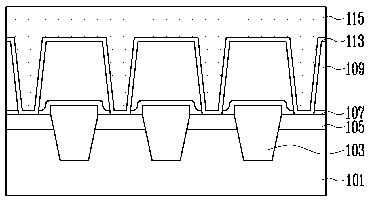
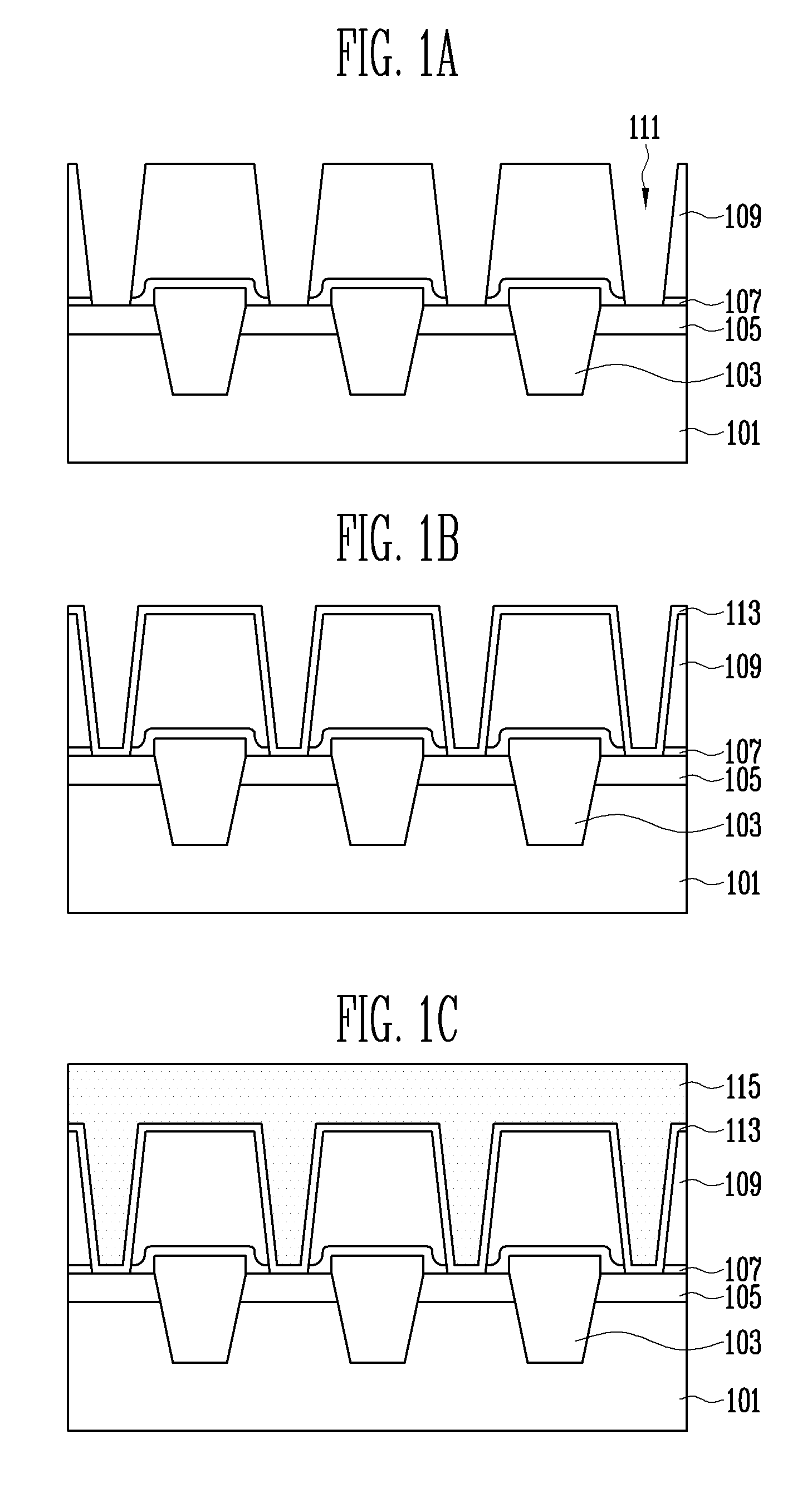
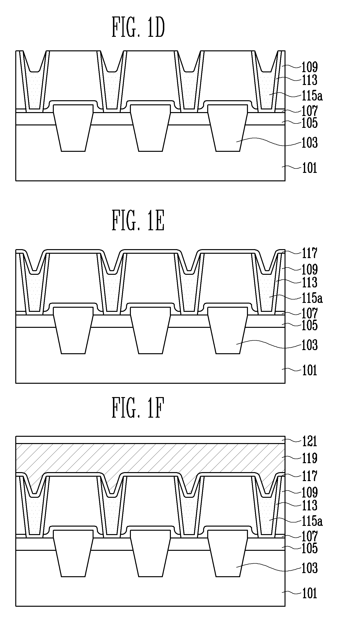
[0029]Referring to FIG. 1A, an isolation layer element 103 is formed on an isolation region element of a semiconductor substrate 101 and a bonding region 105 and a gate (not shown) of a transistor or memory cell are formed on a part of an active region. The isolation layer element 103 is preferably formed in a shallow trench isolation (STI) structure.

[0030]In case of NAND flash memory element, a plurality of the isolation layer elements 103 is formed in parallel on a cell region, and an active region is defined as the semiconductor substrate 101 between the isolation layer elements 103. Additionally, a plurality of word lines and select lines (not shown) is formed on the semiconductor substrate 101 to intersect the isolation layer element 103, and a bonding region 105 is formed on the semiconductor substrate 101 between the ...


PUM


Abstract

According to a method of forming a metal wiring of a semiconductor device, a contact plug is formed at height lower than the contact hole, which is formed on an interlayer insulation layer, and then a metal wiring is formed over the contact plug and interlayer insulation layer to completely fill inside of the contact hole, decreasing process difficulty, ensuring reproducibility, and improving electrical property.

Description

CROSS-REFERENCES TO RELATED APPLICATIONS[0001]The priority of Korean patent application number 10-2007-90290, filed on Sep. 6, 2007, is hereby claimed and its disclosure is incorporated by reference herein in its entirety.BACKGROUND OF THE INVENTION[0002]The present invention relates to a metal wiring of a semiconductor device and method of forming the same, and more particularly to a metal wiring of a semiconductor device and method of forming the same with low resistance, improving electrical characteristics.[0003]Typically, a metal wiring is formed on a semiconductor device for electrically connecting a transistor or memory cell formed on a semiconductor substrate to peripheral circuits. The metal wiring is formed over an interlayer insulation layer and connected to the transistor or peripheral circuits through a contact plug. A contact hole is formed on the interlayer insulation layer and then the contact plug is formed within the contact hole. As the degree of integration of se...

Claims


Application Information

Patent Timeline
Patent Type & Authority Applications(United States)
IPC IPC(8): H01L23/522H01L21/768
CPCH01L21/76877H01L21/76885H01L23/485H01L27/11521H01L2924/0002H01L27/11531H01L2924/00H10B41/42H10B41/30H10B41/35H01L21/28
Inventor KIM, EUN SOOJEONG, CHEOL MOHONG, SEUNG HEE
Owner SK HYNIX INC
Why Eureka
Try Eureka