Method of producing a light-emitting diode comprising a nanostructured PN junction and diode thus obtained

a technology of nanostructured pn junction and light-emitting diodes, which is applied in the direction of nanotechnology, electrical apparatus, semiconductor devices, etc., can solve the problems of preventing the use of integrated light sources, in particular laser lasing mediums, and none of these approaches have enabled current injection to achieve the population, and achieves the effect of easy production

Inactive Publication Date: 2009-03-19
COMMISSARIAT A LENERGIE ATOMIQUE ET AUX ENERGIES ALTERNATIVES
View PDF4 Cites 46 Cited by
  • Summary
  • Abstract
  • Description
  • Claims
  • Application Information

AI Technical Summary

Benefits of technology

[0017]It is a further object of the invention to provide a nanostructured pn junction light-emitting diode, that is easy to produce and is reliable.

Problems solved by technology

However, the indirect energy bandgap of bulk monocrystalline silicon does not enable the latter to be an efficient light emitter and prevents its use as integrated light source, in particular as lasing medium of laser.
Moreover, none of these approaches has enabled current injection to be used to achieve the population inversion necessary to obtain stimulated emission in silicon.
Although a nanostructured silicon pn junction diode can be used as integrated light source, its fabrication method does however remain difficult to implement.
Non-uniform diffusion of the dopant at the substrate surface is also difficult to control, which makes the formation and size of the p+-doped regions, and therefore of the pn junctions, difficult to control.
Moreover, the non-uniform diffusion step and the annealing step are generally performed in separate chambers, which can give rise to diode contamination problems when going from one chamber to the other.
In addition, the annealing step, performed at about 1000° C., for in general a time of 30 minutes, requires a large thermal budget.

Method used


Image

  • Method of producing a light-emitting diode comprising a nanostructured PN junction and diode thus obtained
  • Method of producing a light-emitting diode comprising a nanostructured PN junction and diode thus obtained
  • Method of producing a light-emitting diode comprising a nanostructured PN junction and diode thus obtained

Examples


Embodiment Construction

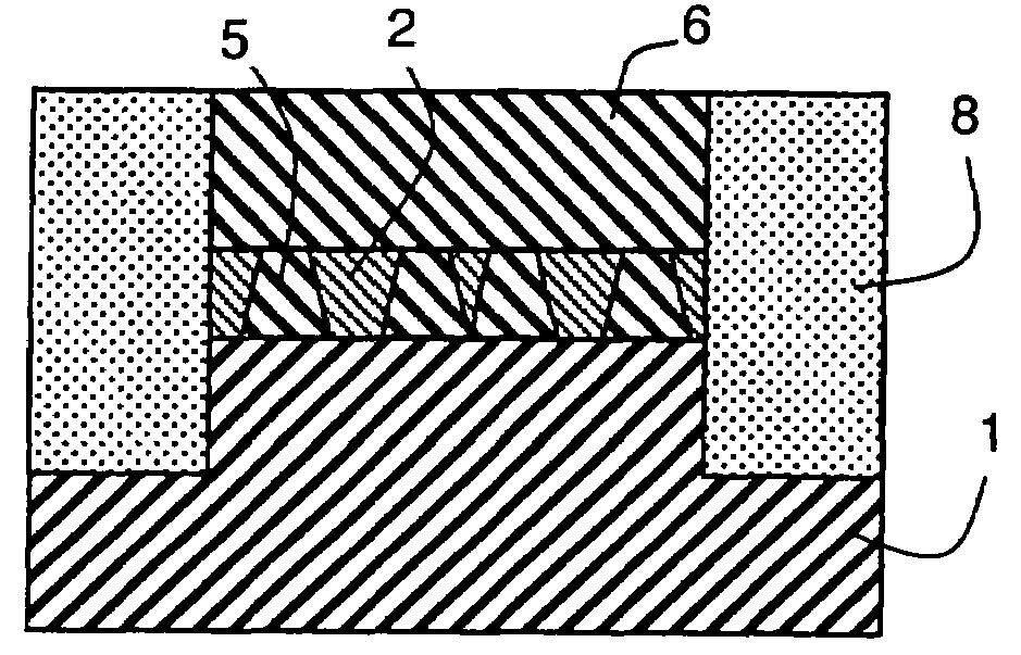
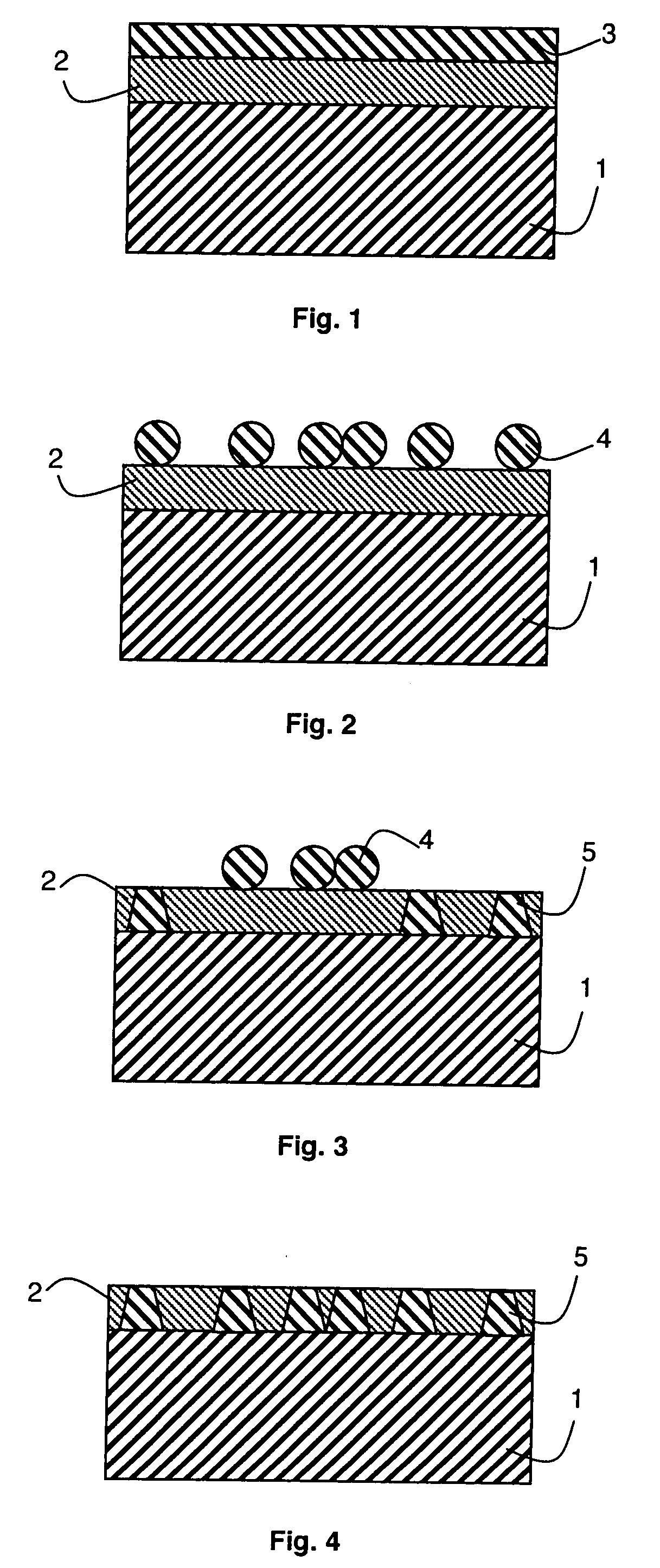
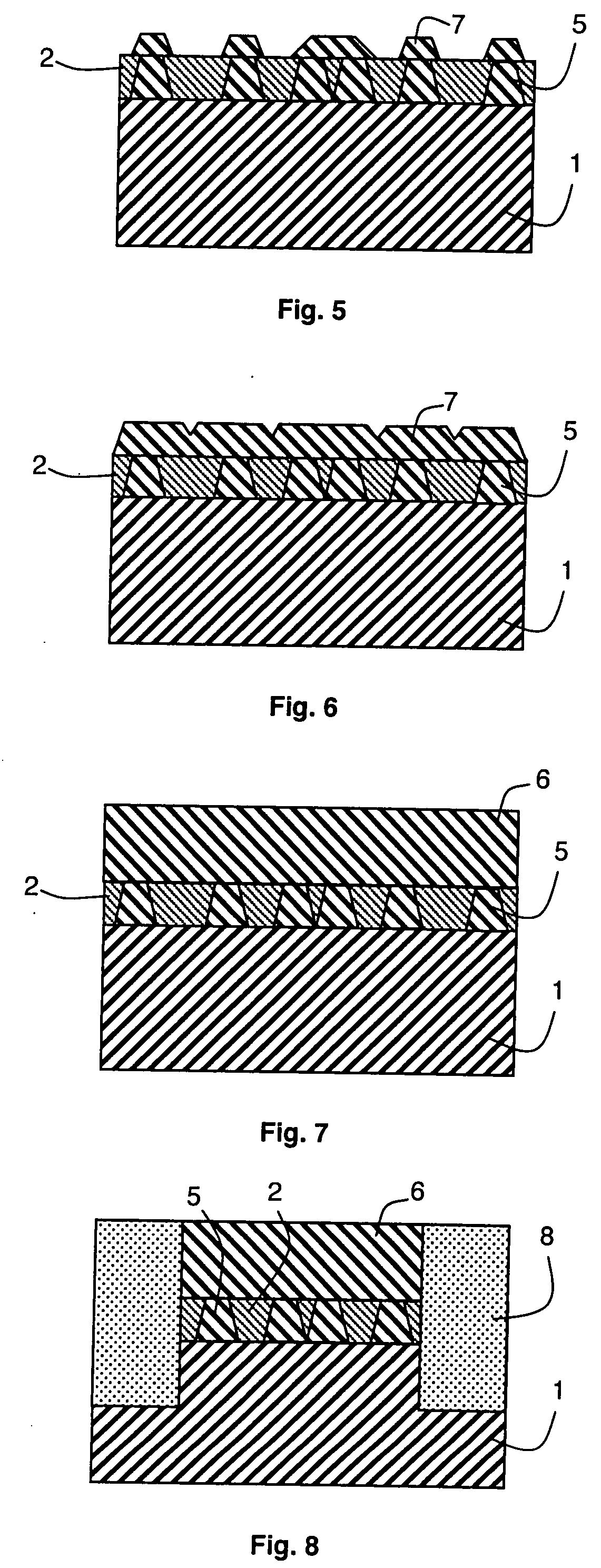
[0024]According to a particular embodiment represented in FIGS. 1 to 9, a nanostructured pn junction light-emitting diode is achieved from a semi-conducting substrate 1 doped by a first dopant and covered by a dielectric thin layer 2. The substrate is, for example, a bulk silicon substrate doped by an n-type dopant such as arsenic or phosphorus. The dielectric thin layer 2 is preferably formed by a thermally decomposable component and, more particularly, decomposable by the effect of a temperature comprised between 720° C. and 750° C. The decomposable component is, for example, chosen from silicon oxide and silicon nitride. The dielectric thin layer 2 preferably has a thickness of about a few nanometers. The thickness of the dielectric thin layer 2 is for example 2 nm.

[0025]As represented in FIG. 1, an amorphous thin film 3 is deposited on the surface of the dielectric thin layer 2 at a temperature preferably lower than or equal to 250° C.

[0026]The amorphous thin film 3 is formed by...


PUM

PropertyMeasurementUnit
temperatureaaaaaaaaaa

Abstract

A nanostructured pn junction light-emitting diode is fabricated from a semi-conducting substrate doped by a first dopant and covered by a dielectric thin layer. An amorphous thin film formed by a semi-conducting material doped by a second dopant of opposite type to that of the first dopant is then deposited on the surface of the dielectric thin layer. The assembly then undergoes a thermal treatment designed to form, in the dielectric thin layer and from the amorphous thin film, a plurality of dots of nanometric size and made of semi-conducting material doped by the second dopant. The dots are designed to be in epitaxial relationship with the substrate to form a plurality of pn junctions of nanometric size. An additional thin layer is then formed by epitaxial growth from the dots.

Description

BACKGROUND OF THE INVENTION[0001]The invention relates to a method for producing a nanostructured pn junction light-emitting diode comprising a semi-conducting substrate doped by a first dopant.[0002]The invention also relates to a nanostructured pn junction light-emitting diode obtained by such a method.STATE OF THE ART[0003]Silicon being the most widely used semi-conducting material in the micro-electronics industry, fabricating opto-electronic integrated circuits with a silicon substrate would be particularly advantageous, in particular to reduce the manufacturing costs of such integrated circuits. This would also enable the technological knowledge derived from the silicon technology to be used to advantage in opto-electronic applications. However, the indirect energy bandgap of bulk monocrystalline silicon does not enable the latter to be an efficient light emitter and prevents its use as integrated light source, in particular as lasing medium of laser.[0004]Different approaches...

Claims


Application Information

Patent Timeline
Patent Type & Authority Applications(United States)
IPC IPC(8): H01L27/15H01L21/00
CPCB82Y10/00H01L21/02381H01L21/02488H01L21/02601H01L21/02532H01L21/02573H01L21/02513Y10S977/774Y10S977/932
Inventor NOE, PIERREMAZEN, FREDERIC
Owner COMMISSARIAT A LENERGIE ATOMIQUE ET AUX ENERGIES ALTERNATIVES
Why Eureka
Try Eureka