Multi-layer ceramic capacitor and manufacturing method of multi-layer ceramic capacitor

a manufacturing method and ceramic capacitor technology, applied in the direction of fixed capacitors, stacked capacitors, fixed capacitor details, etc., can solve the problem of further lowering of the permittivity with respect to the volumic ratio, and achieve the effect of stable production and no remarkable lowering of the permittivity

Active Publication Date: 2009-03-19
TAIYO YUDEN KK
View PDF3 Cites 11 Cited by
  • Summary
  • Abstract
  • Description
  • Claims
  • Application Information

AI Technical Summary

Benefits of technology

[0034]Accordingly, the volumic ratio (vol %) of the Si oxide precipitated to the crystal grain boundary and the grain boundary triple point of the ceramic dielectric layer can be suppressed. This can provide a method of manufacturing a multi-layer ceramic capacitor capable of stable production with no remarkable lowering of the permittivity,

Problems solved by technology

Accordingly, this involves a problem that the glass phase is precipitated to the crystal grain boundary in the ceramic dielectric layer by the addition of the Si oxide to exert compressive stresses on a plurality of ceramic crystal grains constituting the ceramic dielectric layer thereby lowering the permittivity further with respect to the volumic ratio of the crystal grain boundary.

Method used


Image

  • Multi-layer ceramic capacitor and manufacturing method of multi-layer ceramic capacitor
  • Multi-layer ceramic capacitor and manufacturing method of multi-layer ceramic capacitor
  • Multi-layer ceramic capacitor and manufacturing method of multi-layer ceramic capacitor

Examples


examples

[0070]The present invention is to be described based on more specific examples.

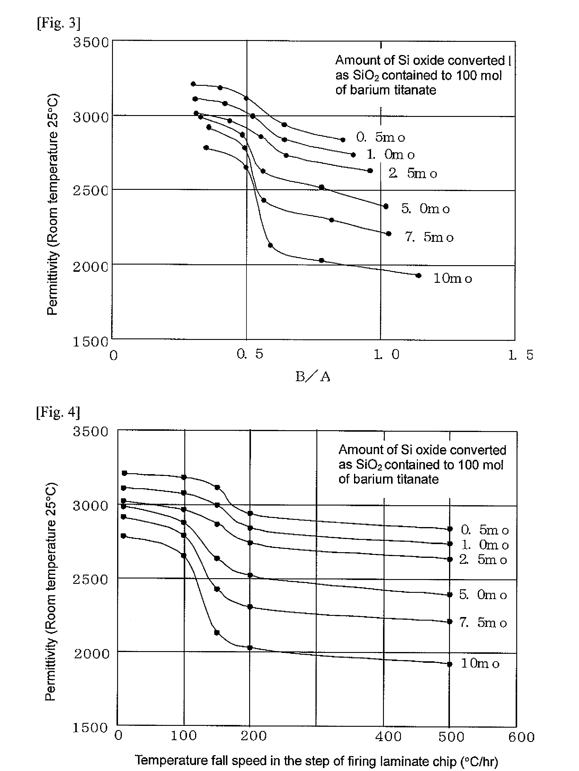
[0071]At first, based on 100 mol of barium titanate with a average grain size of 0.2 μm, starting materials are weighed so as to provide a composition of 1 mol of Ho2O3, 0.5 mol of MgO, 0.1 mol of Mn2O3, 0.5, 1.0, 2.5, 5.0, 7.5, and 10.0 mol each of SiO2, all per 100 mol of barium titanate. These components are wet mixed in a ball mill and then dried to obtain a mixture.

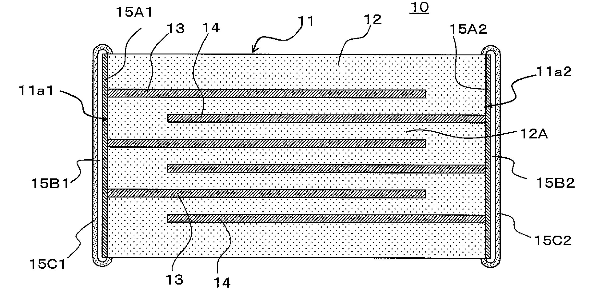
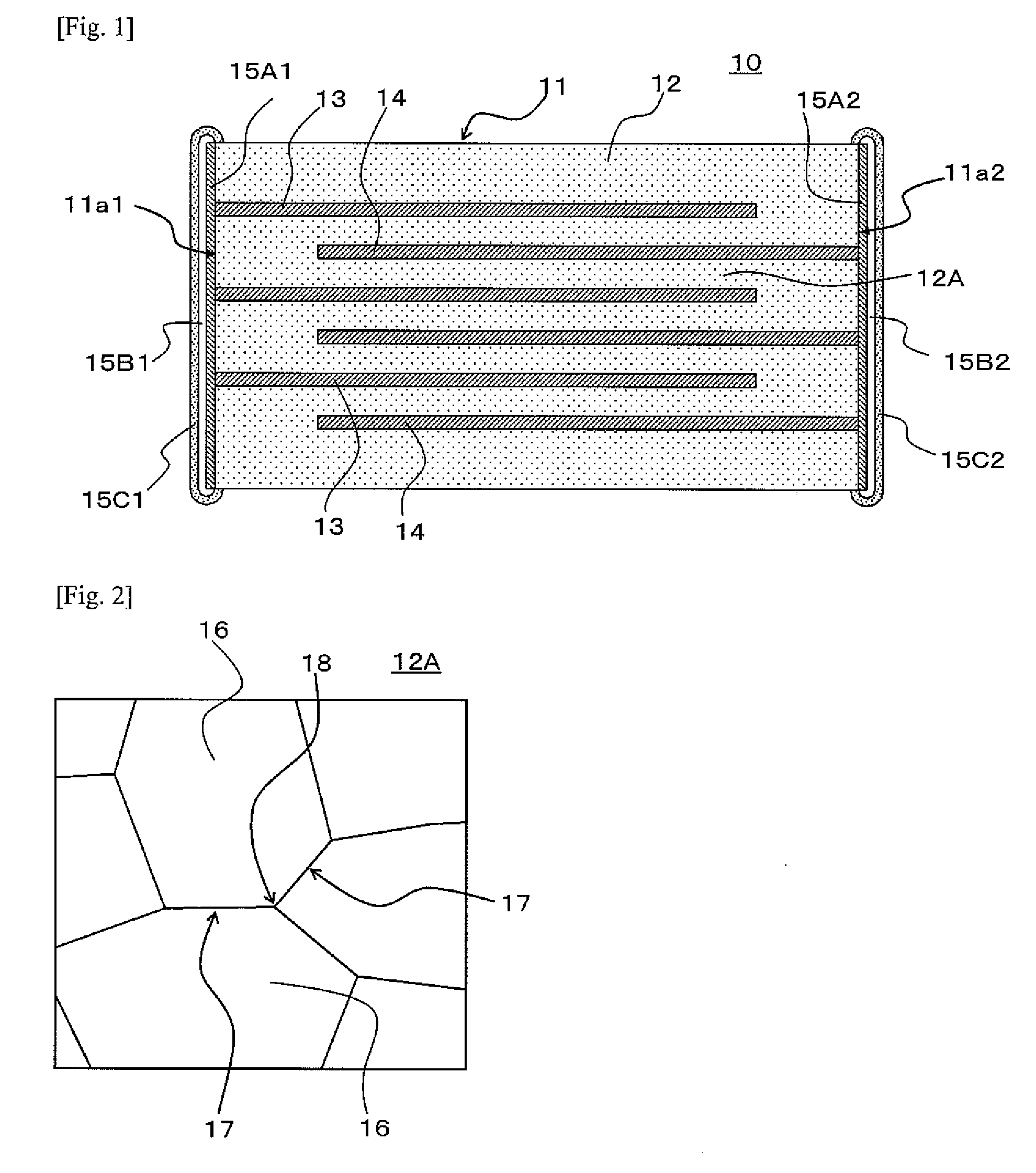
[0072]A slurry is prepared by adding an organic binder and a solvent to the obtained mixture and the obtained slurry is sheeted by a doctor blade method to obtain a sheet of about 1.0 μm thickness. An Ni electrode material paste is coated on the surface of the obtained sheet by screen printing to a thickness of about 1.0 μm to form an internal electrode pattern. Sheets are laminated by 100 layers, and protection sheets are laminated above and below them and crimped under heating to obtain a laminate.

[0073]The obtained laminate is cut such ...


PUM

PropertyMeasurementUnit
sizeaaaaaaaaaa
thicknessaaaaaaaaaa
thicknessaaaaaaaaaa

Abstract

A small, large-capacitance multi-layer ceramic capacitor suppressed for remarkable lowering of permittivity, having a capacitor main body formed of ceramic dielectric layers comprising barium titanate as a main component and an Si oxide at a ratio of 0.5 to 10 mol being converted as SiO2 based on 100 mol of barium titanate and internal electrode layers, and a pair of external electrodes which are formed at the end faces of the capacitor main body and connected electrically with the internal electrode layers, in which the ceramic dielectric layer has crystal grains, crystal grain boundaries each present between the crystal grains and a grain boundary triple point, and B/A is 0.5 or less assuming the amount (mol) of an Si oxide being converted as SiO2 contained based on 100 mol of barium titanate as A and the volumic rate (vol %) of the Si oxide present at the crystal grain boundary and the grain boundary triple point of the ceramic dielectric layer as B, whereby remarkable lowering of a permittivity due to precipitation of an Si oxide to the crystal grain boundary and the grain boundary triple point is suppressed.

Description

PRIORITY[0001]This application claims priority to Japanese Patent Application No. 208659 / 2007, filed Aug. 9, 2007, which is hereby incorporated by reference in its entirety.BACKGROUND OF THE INVENTION[0002]1. Field of the Invention[0003]The present invention concerns a small, large-capacitance multi-layer ceramic capacitor.[0004]2. Description of the Related Art[0005]Japanese Unexamined Publication No. 2006-287045 proposes to provide an electronic part having ceramic dielectric layers comprising barium titanate as a main component such as a multi-layer ceramic capacitor excellent in electric characteristic, excellent in temperature characteristic even in a case of reducing the thickness of the ceramic dielectric layer, having high reliability, reduced in the size and of large capacitance, by controlling the ratio of ceramic particles having a thickness of the crystal grain boundary present between adjacent ceramic crystal grains of 1 nm or less, among a plurality of ceramic particle...

Claims


Application Information

Patent Timeline
Patent Type & Authority Applications(United States)
IPC IPC(8): C04B35/462B32B37/15H01G4/12
CPCC04B35/4682H01G4/30C04B2235/3206C04B2235/3224C04B2235/3225C04B2235/3265C04B2235/3418C04B2235/5445C04B2235/6025C04B2235/6562C04B2235/6565C04B2235/6582C04B2235/663C04B2235/79C04B2235/85H01G4/1227C04B35/638
Inventor TANIGUCHI, KATSUYA
Owner TAIYO YUDEN KK
Why Eureka
Try Eureka