Sheet-Like Underfill Material and Semiconductor Device Manufacturing Method

a technology of semiconductor devices and underfill materials, which is applied in the direction of layered products, transportation and packaging, chemistry apparatus and processes, etc., can solve the problems of undesirably cured heat curing resin, undesirably increased load at a local area of the wafer, and difficulty in operation

Inactive Publication Date: 2009-03-19
LINTEC CORP
View PDF4 Cites 47 Cited by
  • Summary
  • Abstract
  • Description
  • Claims
  • Application Information

AI Technical Summary

Benefits of technology

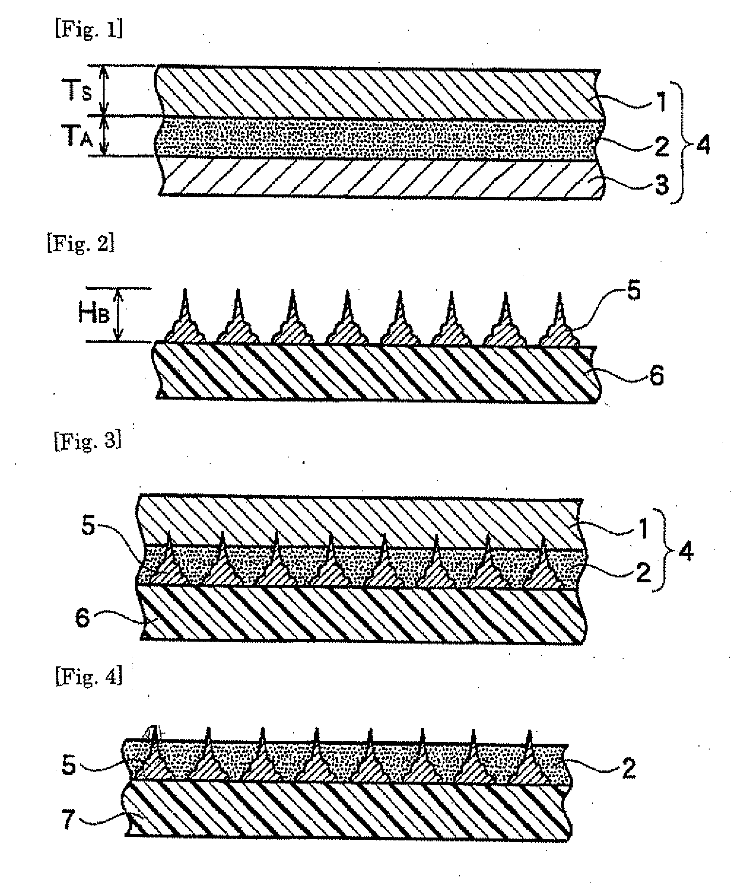
[0026]According to the sheet-like underfill material of the present invention which is applicable to flip chip mounting and the semiconductor device utilizing the same, the underfill can be simply formed on a semiconductor wafer having bumps without precisely controlling the temperature and pressure. Further, even when the bumps are stud bumps, voids are not formed around the roots of the bumps and the like.

Problems solved by technology

Accordingly, the operation may become difficult since the temperature and the pressure greatly affect the fluidity of the resin layer.
For example, when the temperature is elevated for fluidity increase purposes, the heat curing resin is undesirably cured.
On the other hand, increasing the pressure results in undesirably increased load at a local area of the wafer where the bumps are formed.
Further, in the stud bumps, the height of the bump is larger than the diameter of the bump, and, thus, the stud bumps are disadvantageous in that the tops of the bumps are likely to be broken, and, further, air is likely to be caught up in roots of the bumps, leading to a fear of void formation.

Method used


Image

  • Sheet-Like Underfill Material and Semiconductor Device Manufacturing Method
  • Sheet-Like Underfill Material and Semiconductor Device Manufacturing Method

Examples


example 1

[0099]20 parts by weight of (A1), 80 parts by weight of (B), 2 parts by weight of (C), 10 parts by weight of (D), 0.3 part by weight of (E), and 0.3 part by weight of (F) of above components were mixed (in terms of solid weight ratio) together, and methyl ethyl ketone was mixed therein so as to have a solid content of 55% to prepare a HPSA composition. The HPSA composition was coated onto release treated face of a release film (SP-PET 3811, thickness 38 μm, manufactured by Lintec Corporation) so as to have a coating thickness of 50 μm on a dry basis, and the coating was dried at 100° C. for one min. Next, the assembly was laminated onto a low-density polyethylene film (thickness 110 μm, surface tension 34 mN / m) to prepare a sheet-like underfill material.

example 2

[0100]40 parts by weight of (A2), 80 parts by weight of (B), 2 parts by weight of (C), 10 parts by weight of (D), 0.3 part by weight of (E), and 0.3 part by weight of (F) of above components were mixed (in terms of solid weight ratio) together, and methyl ethyl ketone was mixed therein so as to have a solid content of 55% to prepare a HPSA composition. The HPSA composition was coated onto release treated face of a release film (SP-PET 3811) so as to have a coating thickness of 50 μm on a dry basis, and the coating was dried at 100° C. for one min. Next, the assembly was laminated onto a low-density polyethylene film (thickness 110 μm) to prepare a sheet-like underfill material.

example 3

[0101]20 parts by weight of (A2), 80 parts by weight of (B), 2 parts by weight of (C), 5 parts by weight of (D), 0.15 part by weight of (E), and 0.3 part by weight of (F) of above components were mixed (in terms of solid weight ratio) together, and methyl ethyl ketone was mixed therein so as to have a solid content of 55% to prepare a HPSA composition. The HPSA composition was coated onto release treated face of a release film (SP-PET 3811) so as to have a coating thickness of 50 μm on a dry basis, and the coating was dried at 100° C. for one min. Next, the assembly was laminated onto a low-density polyethylene film (thickness 110 μm) to prepare a sheet-like underfill material.


PUM

PropertyMeasurementUnit
Young's modulusaaaaaaaaaa

Abstract

A sheet-like underfill material includes a base and adhesive layer provided peelably on the base for use in a flip chip mounting process in the manufacture of a semiconductor device. The process includes laminating a sheet-like underfill material onto a circuit face of a semiconductor wafer having bumps on its circuit face and, simultaneously, allowing the bumps to pierce the adhesive layer and allowing the tops of the bumps to penetrate the base. The base has a storage elastic modulus of 1.0×10⁶ Pa to 4.0×10⁹ Pa, a breaking stress of 1.0×10⁵ Pa to 2.0×10⁸ Pa, and a Young's modulus of 1.0×10⁷ Pa to 1.1×10¹⁰ Pa. The adhesive layer has a storage elastic modulus of 1.0×10⁴ Pa to 1.0×10⁷ Pa and a breaking stress of 1.0×10³ Pa to 3.0×10⁷ Pa.

Description

TECHNICAL FIELD[0001]The present invention relates to a sheet-like underfill material for use in flip chip mounting and a process for producing a semiconductor device using the same.BACKGROUND ART[0002]For mounting multipin LSI packages to prepare MPUs, gate arrays or the like onto printed wiring boards, a flip chip mounting method has hitherto been adopted in which convex electrodes (bumps) made of eutectic solder, high-temperature solder, gold or the like are formed on a connection pad part of a semiconductor chip and are confronted with and are brought into contact with corresponding terminal parts on a chip mounting substrate by the so-called “facedown method” for melt / diffusion bonding. In this method, however, there is a fear that, upon exposure to a periodical temperature fluctuation, the joint is broken due to a difference in coefficient of thermal expansion between the semiconductor chip and the chip mounting substrate. To overcome this problem, a method has been proposed i...

Claims


Application Information

Patent Timeline
Patent Type & Authority Applications(United States)
IPC IPC(8): H01L21/50B32B7/12
CPCH01L21/563Y10T428/2839H01L23/293H01L24/12H01L2224/1134H01L2224/131H01L2224/13144H01L2224/16H01L2224/274H01L2224/83191H01L2924/01004H01L2924/01025H01L2924/01079H01L21/6835H01L2224/81191H01L2924/07802H01L2224/73104H01L2224/27436H01L24/27H01L2924/01322H01L2924/01019H01L2924/00013H01L2924/014H01L2924/00014H01L2224/13099H01L2924/3512H01L2924/00H01L2924/351H01L23/29
Inventor SATO, AKINORIYAMAZAKI, OSAMUTAKAHASHI, KAZUHIRO
Owner LINTEC CORP
Why Eureka
Try Eureka