Method of attaching an electronic device to an mlcc having a curved surface

Active Publication Date: 2009-03-26
KEMET ELECTRONICS
View PDF9 Cites 13 Cited by
  • Summary
  • Abstract
  • Description
  • Claims
  • Application Information

AI Technical Summary

Benefits of technology

[0019]Yet another advantage is provided in a method of forming an electrical connection. The method includes providing a substrate wherein the substrate has a mounting surface with a curvature deviation exceeding 0.008 inches per inch. Providing an electronic component. Forming a conductive column on the electronic component wh

Problems solved by technology

This has led to a myriad of problems at every level of circuit design starting with the component design, through component attachment techniques, circuit board design, and the design of the device packaging.
But as size, portability, and increased functionality of electronics became design driving issues, entire assemblies and the components used in them also had to decrease in size.
This trend increases the pressure on packaging, thus forcing the development of new I/C interconnects and packaging technologies that provide continually decreasing fo

Method used


Image

  • Method of attaching an electronic device to an mlcc having a curved surface
  • Method of attaching an electronic device to an mlcc having a curved surface
  • Method of attaching an electronic device to an mlcc having a curved surface

Examples


Example

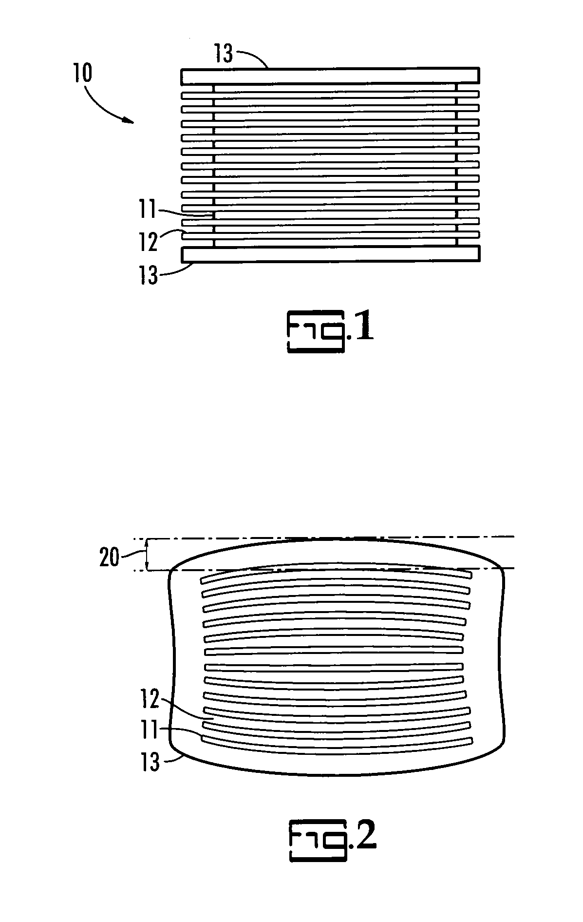
[0050]Provided herein is an improved method for attaching electronic devices to a substrate having a curved surface. More particularly, the present invention provides a method for attaching electronic devices to a substrate with a curvature of more than 0.008 inches per linear inch.

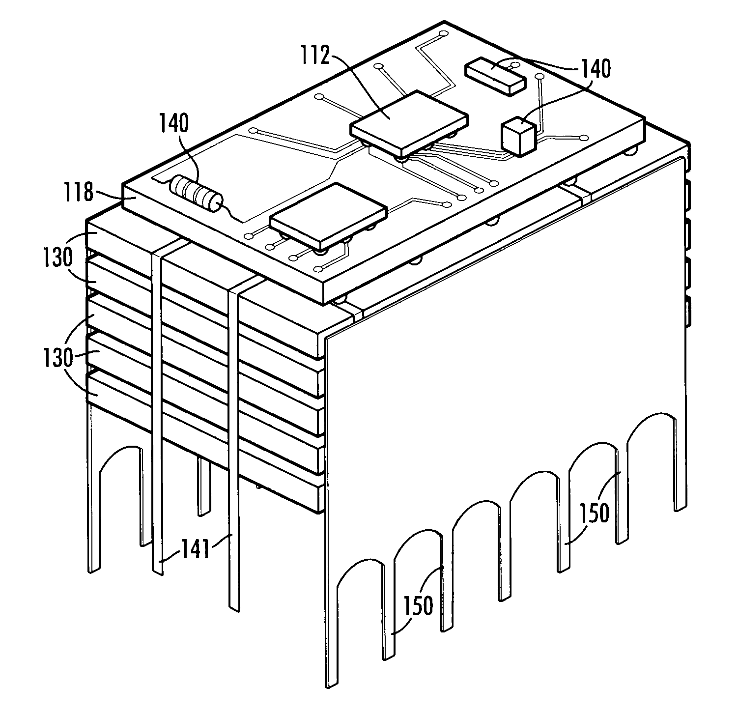
[0051]More particularly, this invention provides a unique solution that utilizes the surface of an MLCC to attach an active I / C onto the surface of the MLCC while integrating the I / C into the active circuitry of the module.

[0052]In one embodiment this invention provides a solution to a problem that exist at the component level by providing a method of mounting an electronic chip to a MLCC having a potential surface curvature in excess of 0.008 inch / linear inch to achieve a mechanically sound and electrically robust bond in a cost effective manner by combining the advantages of Flip Chip technologies with the flexibility of small flex circuits called Re-Distribution Layers, (RDL's).

[0053]The invention will...


PUM

PropertyMeasurementUnit
Fractionaaaaaaaaaa
Dimensionless propertyaaaaaaaaaa
Flexibilityaaaaaaaaaa

Abstract

A method of forming an electrical component is provided. The method comprises preparing a subassembly by electrically connecting an integrated circuit to a flexible circuit; and attaching the subassembly to a multilayer ceramic capacitor having a mounting surface with a curvature deviation exceeding 0.008 inches per inch.

Description

CROSS-REFERENCE TO RELATED APPLICATIONS[0001]This application claims priority to pending U.S. Provisional Patent Appl. No. 60 / 974,594 filed Sep. 24, 2007 which is incorporated herein by reference.BACKGROUND OF THE INVENTION[0002]The present invention is directed to a method of attaching a semiconductor integrated circuit active device to a multi-layer ceramic capacitor (MLCC) having a non parallel and a non-uniform surface as compared to the surface of the Integrated Circuit (I / C), and at the same time, creating additional opportunities for increasing functionality of the MLCC assembly.[0003]The proliferation of smaller, more complex, electronic devices is a never ending trend of the electronics industry. Market dynamics have forced circuit designers to achieve more functionality in less space. This has led to a myriad of problems at every level of circuit design starting with the component design, through component attachment techniques, circuit board design, and the design of the ...

Claims


Application Information

Patent Timeline
IPC IPC(8): H01R43/00
CPCH01G4/12Y10T29/4913H01G4/40H05K1/0306H05K1/141H05K1/147H05K3/4611H05K3/4629H05K2201/09018Y10T29/49117Y10T29/49124Y10T29/49126Y10T29/435Y10T29/49169Y10T29/49144H01G4/30H01L2224/16265H01L2224/16225H01L2924/15311H01L2924/19105H01L2924/19106
Inventor RANDALL, MICHAEL S.WAYNE, CHRISMCCONNELL, JOHN
Owner KEMET ELECTRONICS
Why Eureka
Try Eureka