Semiconductor device

A semiconductor and device technology, which is applied in the field of semiconductor devices, can solve the problems of unstable size and shape of elastomers, unsteady semiconductor chip bonding process, and difficult elastomers, and achieve excellent noise resistance, stable size and shape, and high The effect of yield

Inactive Publication Date: 2006-02-01
HITACHI LTD +1
View PDF0 Cites 8 Cited by
  • Summary
  • Abstract
  • Description
  • Claims
  • Application Information

AI Technical Summary

Problems solved by technology

For example, since the flexible wiring board in the above-mentioned package structure adopts a so-called rear wiring structure in which an elastic body is formed on the wiring surface of the wiring board, the unevenness of the wiring pattern on the flexible wiring board becomes a key factor. It is difficult to overlap the elastomer evenly and stably
[0009] In other words, when coating or affixing the elastic body on the flexible wiring board, air holes that cannot be filled with the elastic body are formed on both sides of the convex part of the wiring pattern, or due to the unstable size and shape of the elastic body, there may be The problem that the bonding process of semiconductor chips cannot be performed stably

Method used


Image

  • Semiconductor device
  • Semiconductor device
  • Semiconductor device

Examples


Embodiment 1

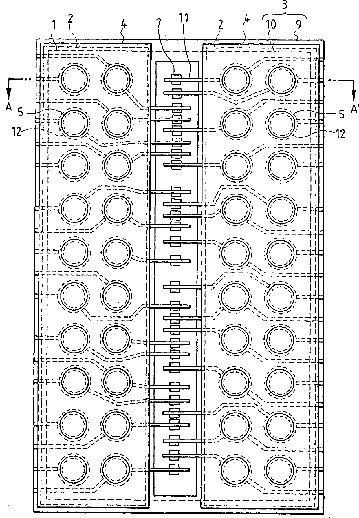
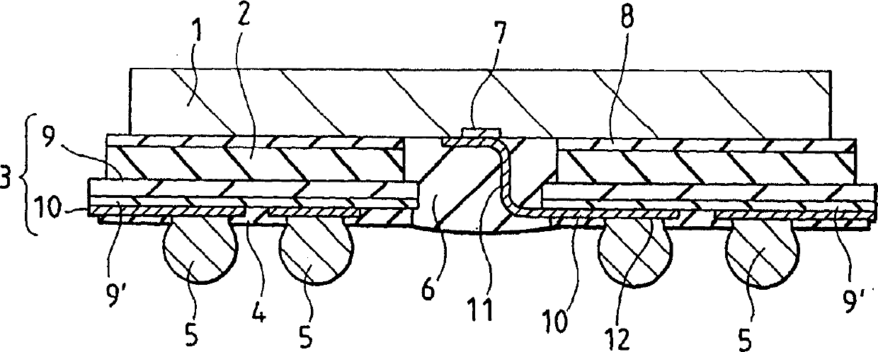
[0156] The plan view of Fig. 1 shows the semiconductor integrated circuit device of Embodiment 1 of the present invention; Fig. 2 is the cross-sectional view at AA' section line place of Fig. 1; The plan view and cross-sectional view of Fig. 3 and Fig. 4 show semiconductor The assembly state of the integrated circuit device assembled on the assembly substrate; what Fig. 5 shows is the flow chart of the assembly process of the semiconductor integrated circuit device; Fig. 6-Fig. 58, Fig. 76-Fig. It is an explanatory diagram for explaining the comparison between the characteristics of the circuit device and the semiconductor integrated circuit device of the comparative example studied by the present inventors. The description of these figures will be described item by item in each technical item described later.

[0157] First, the configuration of the semiconductor integrated circuit device of the first embodiment will be described with reference to FIGS. 1 and 2. FIG.

[0158...

Embodiment 2

[0292] The semiconductor integrated circuit device of this embodiment 2 is the same as the above-mentioned embodiment 1, and it is made into a semiconductor package of a ball grid array type. The difference between the semiconductor integrated circuit device and the above-mentioned embodiment 1 is whether the surface wiring structure is a premise technology. , but is based on the premise of the rear wiring structure and is used to improve it. For example, as shown in Figure 59 and Figure 60, the elastomer 2 that has been bonded to the main surface of the semiconductor chip 1 and will be In the structure between the flexible wiring board 3 (wiring board) on the main surface of the elastic body 2 , a solder resist layer 56 (insulating film) has been formed on the back surface of the flexible wiring board 3 .

[0293] That is, the flexible wiring substrate 3 becomes composed of the substrate base material 9 to be the base material of the flexible wiring substrate 3 and the wiring ...

Embodiment 3

[0302] 63 is a plan view of a semiconductor integrated circuit device as Embodiment 3 of the present invention viewed from the back of the semiconductor chip; FIG. 62 is a plan view; FIG. 63 is a sectional view; FIG. 64 is an enlarged sectional view of part A of FIG. 63; FIG. 65 It is a plan view for explaining the wiring structure of the wiring board.

[0303] The semiconductor integrated circuit device of this embodiment 3 does not use the semiconductor package with the so-called fan-in central pad structure of the above-mentioned embodiments 1 and 2, but instead uses a peripheral pad structure as shown in Figures 61-65. In the semiconductor chip 1a, the solder bumps 5a connected to the bonding pads of the semiconductor chip 1a are arranged on the area inside from the outer circumference of the semiconductor chip 1a to form a so-called fan-in peripheral pad. Package construction. Also, even in this embodiment 3. It also becomes each technical item that has already adopted ...


PUM

PropertyMeasurementUnit
thicknessaaaaaaaaaa

Abstract

A ball grid array type semiconductor package includes a semiconductor chip formed with bonding pads, an elastomer bonded to the semiconductor chip, a flexible wiring substrate bonded to the elastomer and formed with wirings connected at one end of the bonding pads of the semiconductor chip, a solder resist formed on the main surface of the flexible wiring substrate and solder bump electrodes connected to the other ends of the wirings. The elastomer is bonded to the flexible wiring substrate on the side of the tape, the solder resist is formed on the side of the wirings, and the solder bump electrodes are connected with the wirings by way of through holes formed in the solder resist.

Description

[0001] This application is a divisional application of an invention patent application with a filing date of March 21, 1997, an application number of 97104876.2, and an invention title of "semiconductor integrated circuit device and its manufacturing method". technical field [0002] The present invention relates to a semiconductor device, and in particular to a technology applicable and effective to portable devices such as mobile phones and portable personal computers, which have been active in the direction of small size, light weight, and thinning. Background technique [0003] In recent years, there has been active movement towards higher functionality, higher performance, smaller size, lighter weight, and thinner electronic devices. In this regard, the recent rapid increase in portable devices such as portable telephones and portable personal computers plays a large role. In addition, the function of the human-machine interface of the machine operated by an individual ...

Claims


Application Information

Patent Timeline
Patent Type & Authority Applications(China)
IPC IPC(8): H01L23/488H01L21/60H01L21/50H01L21/98H01L23/12H01L23/28H01L23/48H01L23/495H01L23/498H01L23/50H01L27/105
CPCH01L2924/01015H01L23/4985H01L2924/01023H01L2924/0105H01L2924/01082H01L23/49827H01L2924/01004H01L2924/01002H01L2224/73215H01L2924/15311H01L2924/01029H01L2224/0401H01L2224/85951H01L2224/48472H01L2224/06136H01L2924/014H01L2924/01013H01L2224/45147H01L24/06H01L24/48H01L2924/01079H01L2224/48465H01L2224/04042H01L2924/14H01L2924/01005H01L2924/01033H01L2924/01006H01L23/49816H01L2924/01078H01L24/50H01L2924/01014H01L2924/01057H01L2224/45144H01L24/45H01L24/86H01L2224/05554H01L2224/45015H01L2224/45124H01L2224/50H01L2924/00011H01L2924/00014Y10T29/4913Y10T29/49169H01L2924/20753H01L2224/05599H01L23/28
Inventor 宫崎忠一秋山雪治柴本正训下石智明安生一郎西邦彦西村朝雄田中英树木本良辅坪崎邦宏长谷部昭男
Owner HITACHI LTD
Why Eureka
Try Eureka