Three dimensional vertical e-fuse structures and methods of manufacturing the same
- Summary
- Abstract
- Description
- Claims
- Application Information
AI Technical Summary
Benefits of technology
Problems solved by technology
Method used
Image

Examples
first embodiment
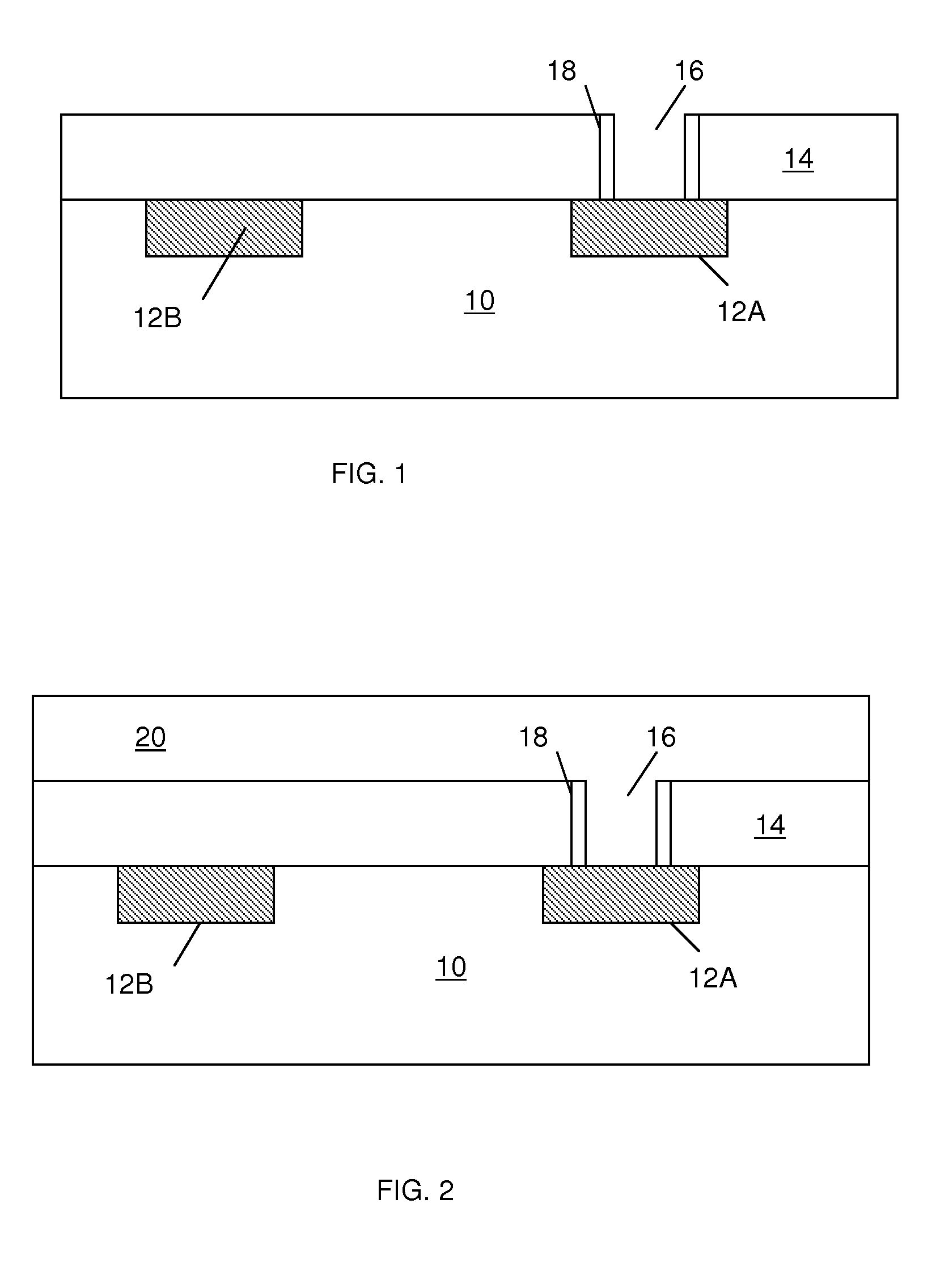
[0020]FIG. 1 shows a beginning structure of an e-fuse structure according to the invention. In this beginning structure, a metallization 12a, 12b, at a first level (M1), is formed in a substrate 10 such as, for example, SiO2. The metallization 12a, 12b may be patterned into the substrate 10 in any known, conventional manner. It is understood that the present invention contemplates more than metallization 12a, 12b at any of the levels (M1, M2, etc.); and that the use of metallization 12a, 12b is provided for non-limiting, illustrative purposes and ease of discussion only. Accordingly, one of skill in the art would recognize that the invention can be implemented with more than two metallization at each layer in accordance with the novel aspects of the invention discussed herein. In embodiments, the metallization 12a, 12b is Copper (Cu); although, any known metal layer is contemplated for use with the invention.
[0021]A layer 14 is formed over the metallization 12a, 2b and substrate 10....
second embodiment
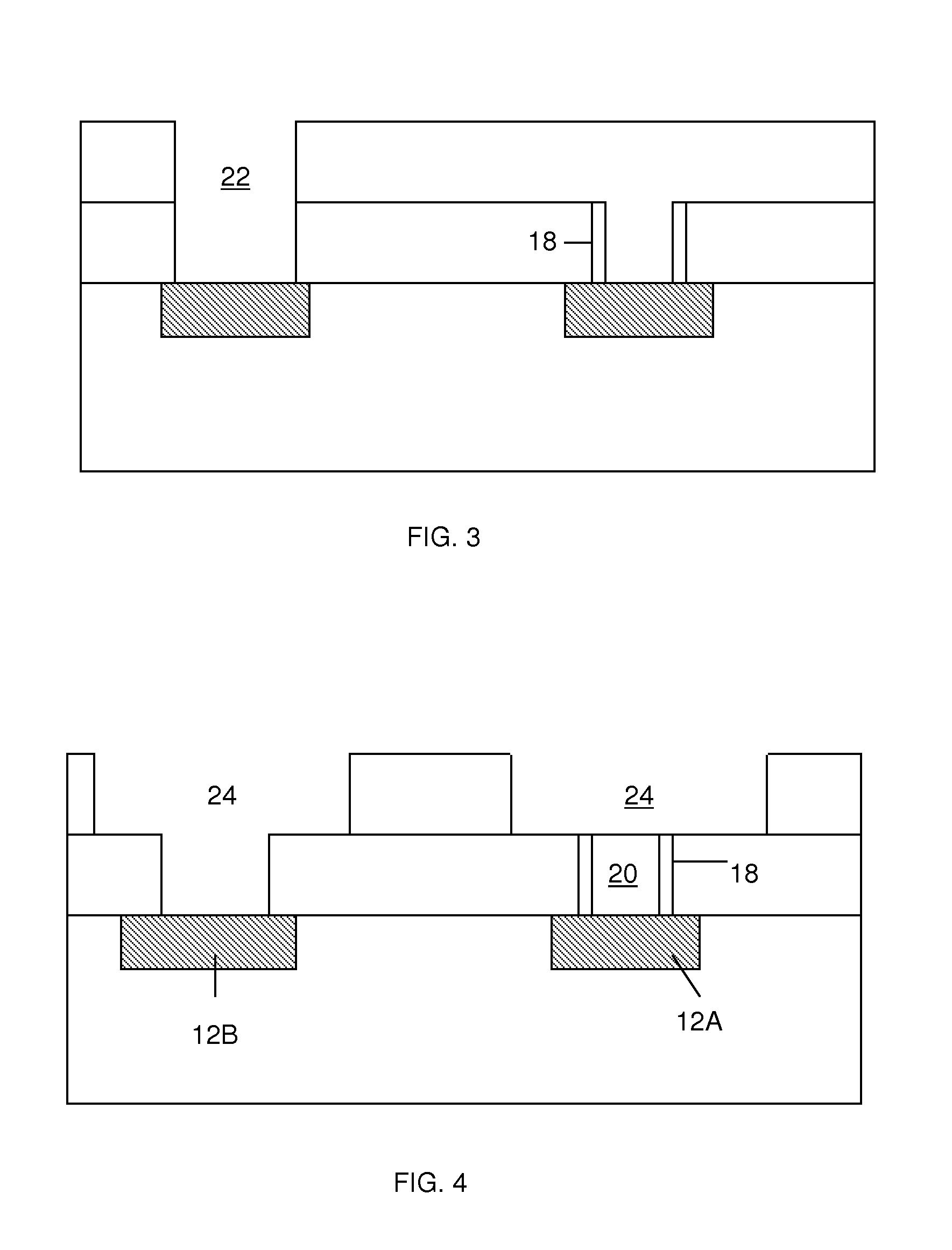
[0025]FIG. 6 shows a beginning structure of an e-fuse structure according to the invention. In the beginning structure of FIG. 6, metallization 12a, 12b is formed at a first level M1 in the substrate 10 in any known, conventional manner. In embodiments, the metallization 12a, 12b is copper (Cu); although, any known metal layer is contemplated for use with the invention. A layer 14 is formed over the metallization 12b and is patterned to form a via over the metallization 12b. The via is filled with metal 28 such as, for example, Cu, which will form an interconnect to metal layer M2. The structure is then planarized using, for example, CMP. The layer 14 may be an insulator comprising SiCOH, SiO2, fluorinated SiO2, or any of a variety of organic low K dielectrics (interlevel dielectric) known to be used in semiconductor fabrication.
[0026]FIGS. 7-9 show fabrication processes of an e-fuse structure according to the second embodiment of the invention. In FIG. 7, a via 16 is formed over at...
third embodiment
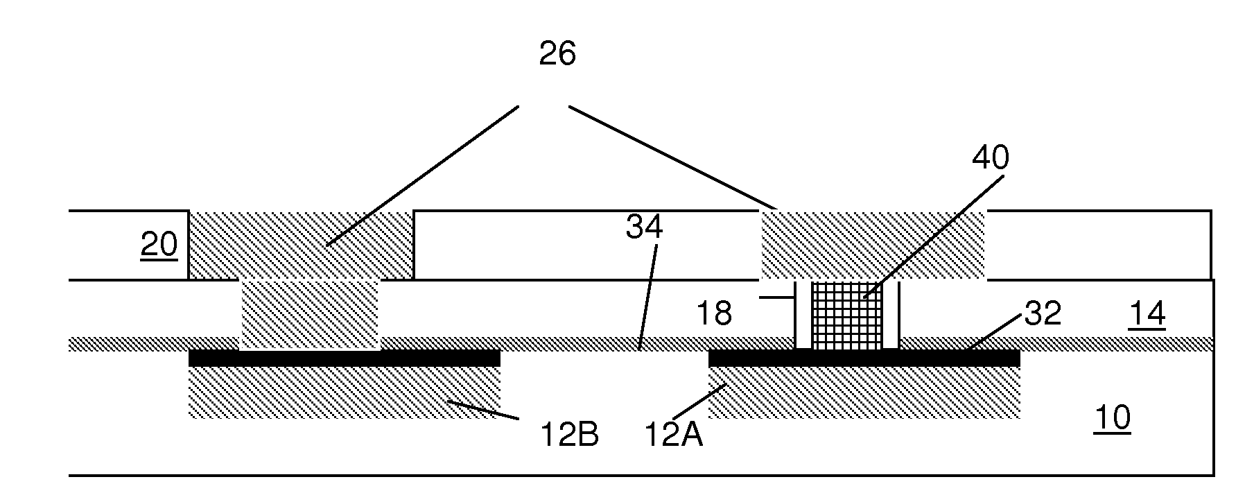
[0029]FIG. 10 shows a beginning structure of an e-fuse structure according to the invention. In this structure, a CoWP layer 32 is formed in contact with the metallization 12a, 12b. In this embodiment, the CoWP layer 32 protects the metal layer (e.g., Cu) during M2 dielectric deposition. A SiN layer 34 is formed over the entire structure. The thin conductive material 18 is provided within an etched pattern of the layer 14, using conventional processes, as discussed above. The layer 14 may be an insulator as discussed above. In this embodiment, the liner 18 may be, for example, NiSi, CoSi2 or TiSi2 or other known conductive materials such as copper. The liner 18 may be between about 10 nm to 200 nm, and preferably about 50 nm, and extends to the CoWP layer 32, which is over the metallization 12a.
[0030]In embodiments, the structure (fuse) of FIG. 10 may be formed by PVD or CVD silicide plus RIE processes. Alternatively, the structure of FIG. 10 may be formed by PVD or CVD Si, plus RI...
PUM
 Abstract
Description
Claims
Application Information
 - Generate Ideas
- Intellectual Property
- Life Sciences
- Materials
- Tech Scout
- Unparalleled Data Quality
- Higher Quality Content
- 60% Fewer Hallucinations
Browse by: Latest US Patents, China's latest patents, Technical Efficacy Thesaurus, Application Domain, Technology Topic, Popular Technical Reports.
© 2025 PatSnap. All rights reserved.Legal|Privacy policy|Modern Slavery Act Transparency Statement|Sitemap|About US| Contact US: help@patsnap.com