Method for manufacturing electroluminescence element

a manufacturing method and technology of electroluminescence elements, applied in the direction of photomechanical devices, instruments, transportation and packaging, etc., can solve the problems of difficult formation of photoresist layers, difficult light emission layer formation, and patterned light emission layers, etc., to achieve efficient transport charges, efficient transfer of exciton energy, and simplified manufacturing process

Active Publication Date: 2009-04-02
DAI NIPPON PRINTING CO LTD
View PDF11 Cites 54 Cited by
  • Summary
  • Abstract
  • Description
  • Claims
  • Application Information

AI Technical Summary

Benefits of technology

[0020]In the present invention, the coating liquid (for formation of each of the light emitting layer and the light emitting layer portions) may further contain at least one of the hole transport material and an electron transport material. A combination of the quantum dots and at least one of the materials makes it possible to simplify the process of manufacturing an EL element, efficiently transport charges into the light emitting layers, and efficiently transfer energy of an exciton generated by a recombination of a hole and an electron. This results in an improvement in the life characteristics of the EL element.
[0021]According to the present invention, before the step of forming the photoresist layer, a coating liquid (for formation of a hole injection layer) containing a hole injection material and a curable binder may be coated on the substrate having the first electrode layer and cured to form the hole injection layer. The formation of the hole injection layer stabilizes injection of holes into the light emitting layer to improve the light emission efficiency.
[0022]According to the present invention, the silane coupling agent may be a silicon compound represented by YnSiX(4−n) (where, Y represents an alkyl group, a fluoroalkyl group, a vinyl group, an amino group, a phenyl group or an epoxy group; X represents an alkoxyl group, an acetyl group or a halogen group; and n represents an integer of 0 to 3). Molecular design of the silicon compound is relatively easy. The groups X and Y are appropriately selected to control condensation of the compound and the like. This makes it possible to obtain desired stability of the quantum dots included in the light emitting layer.
[

Problems solved by technology

The lift-off method can suppress a reduction in performance of the light emitting layer such as light emission characteristics.
It has been, therefore, difficult to form a photoresist lay

Method used


Image

  • Method for manufacturing electroluminescence element
  • Method for manufacturing electroluminescence element
  • Method for manufacturing electroluminescence element

Examples


first embodiment

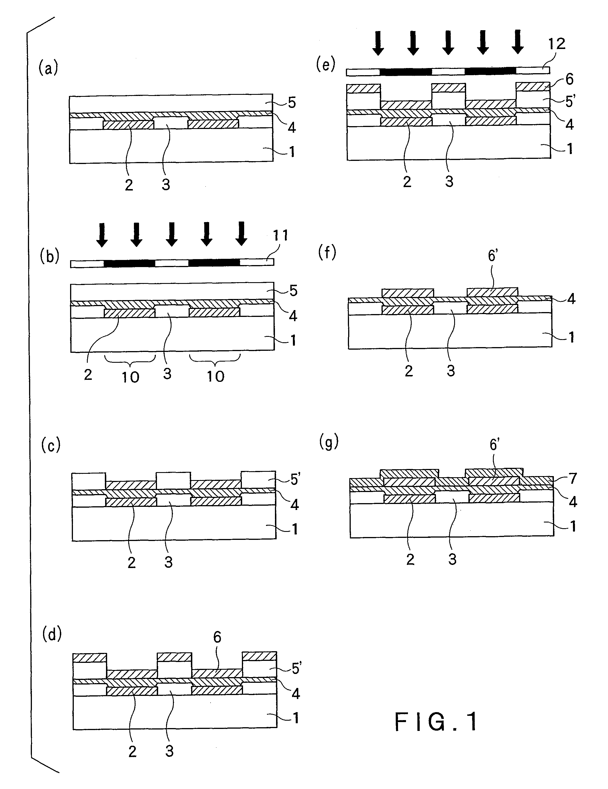
[0034]According to the first embodiment of the present invention, the method for manufacturing an electroluminescence element comprises the steps of: preparing a substrate having a first electrode layer formed thereon; forming a photoresist layer on the substrate having the first electrode layer formed thereon; exposing and developing the photoresist layer, and patterning the photoresist layer to ensure that a portion of the photoresist layer, which is located in a light emission area, is removed; coating a coating liquid on the resultant substrate having the patterned photoresist layer, curing the coating liquid to form a light emitting layer, the coating liquid containing a quantum dot having a silane coupling agent attached to the surface thereof; removing the remaining photoresist layer to lift off a portion of the light emitting layer, which is present on the photoresist layer.

[0035]The method for manufacturing an EL element according to the present embodiment will be described...

first example

(1) FIRST EXAMPLE

[0065]In the process of forming the light emitting layer according to the first example, the coating liquid (for formation of the light emitting layer) containing the quantum dot having the silane coupling agent attached to the surface thereof is coated on the substrate having the photoresist layer patterned, and cured to form the single light emitting layer. The coating liquid (for formation of the light emitting layer) and the method for forming the light emitting layer will be described below.

(i) Coating Liquid for Formation of Light Emitting Layer

[0066]The coating liquid (for formation of the light emitting layer) used in the present embodiment contains the quantum dot having the silane coupling agent attached to the surface of the quantum dot. Typically, the quantum dot having the silane coupling agent attached to the surface thereof is dispersed in a solvent. Materials contained in the coating liquid will be described below.

(Quantum Dot)

[0067]The quantum dot u...

second example

(2) SECOND EXAMPLE

[0107]In the process of forming the light emitting layer according to the second example, the coating liquid (for formation of the light emitting layer) that contains the quantum dot having the silane coupling agent attached to the surface thereof and contains at least one of the hole transport material and an electron transport material is coated on the substrate having the patterned photoresist layer and cured to form the single light emitting layer.

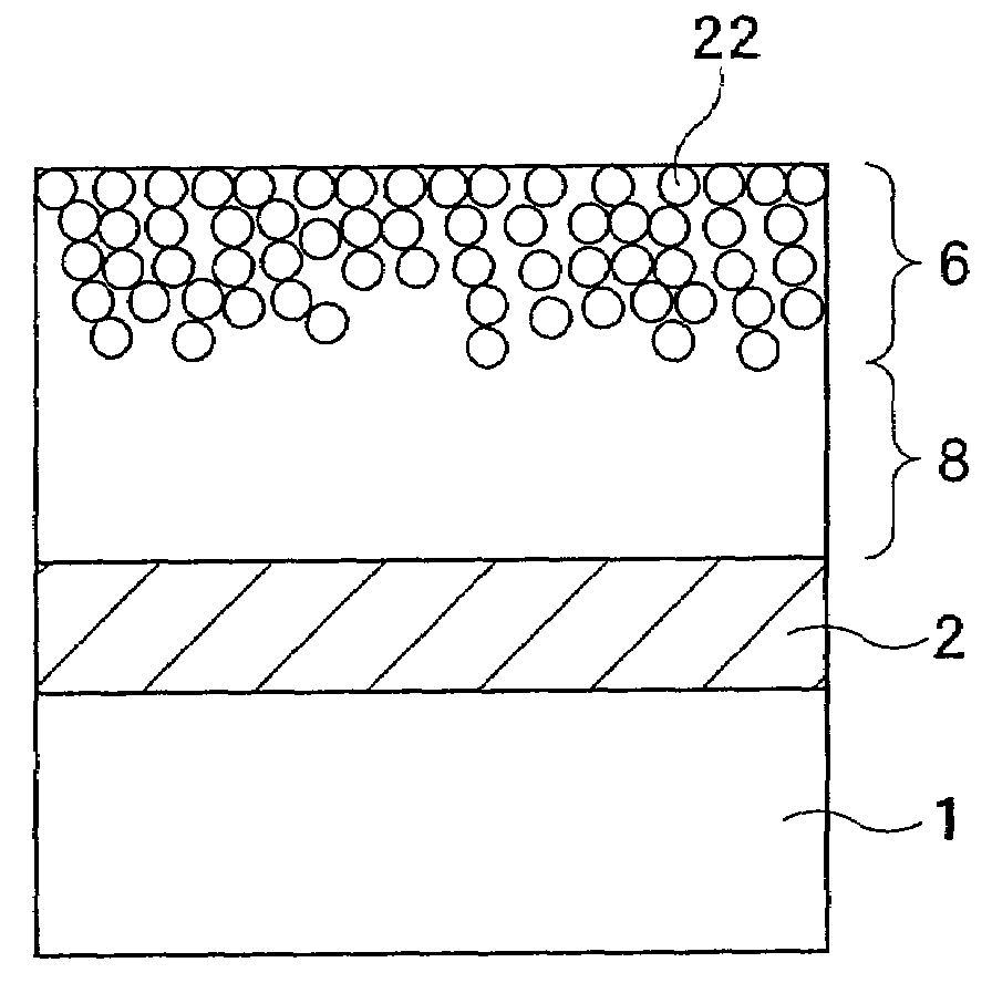
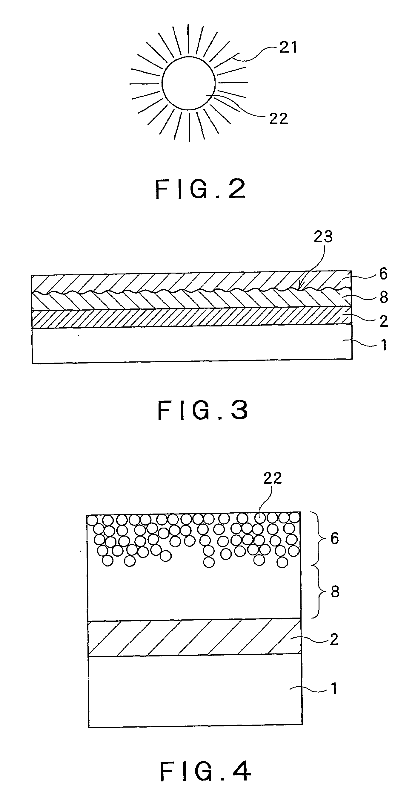
[0108]In the second example, the light emitting layer has not only a function for emitting light but also at least one of a function for transporting a hole and a function for transporting an electron. The process of manufacturing the EL element can therefore be simplified. In addition, The EL element according to the second example is capable of transporting a charge to the light emitting layer and efficiently transferring energy of an exciton generated by recombination of a hole and an electron. The life characteris...


PUM

PropertyMeasurementUnit
Coloraaaaaaaaaa
Band gapaaaaaaaaaa
Transport propertiesaaaaaaaaaa

Abstract

The present invention provides a method for manufacturing an electroluminescence element that has a light emitting layer containing a quantum dot and exhibits excellent life characteristics. In the method, patterning of the light emitting layer can be stably performed by a lift-off method. A photoresist layer is formed on a substrate having a first electrode layer. The photoresist layer is then exposed, developed, and patterned to ensure that a portion of the photoresist layer, which is located in a light emission area, is removed. A coating liquid containing a quantum dot having a silane coupling agent attached to the surface thereof is coated on the resultant substrate having the patterned photoresist layer and cured to form a light emitting layer. The remaining photoresist layer is then removed to lift off a portion of the light emitting layer, which is present on the photoresist layer.

Description

CROSS-REFERENCE TO RELATED APPLICATIONS[0001]The present application benefits from Japanese application JP2007-256588, filed on Sep. 28, 2007, the disclosure of which is hereby incorporated by reference in its entirety.BACKGROUND OF THE INVENTION[0002]1. Field of the Invention[0003]The present invention relates to a method for manufacturing an electroluminescence element (hereinafter also called an EL element in some cases) having a light emitting layer that contains a quantum dot and is formed by photolithography.[0004]2. Description of the Related Art[0005]In an EL element, a hole injected from one of two electrodes facing each other and an electron injected from the other of the electrodes are coupled in a light emitting layer; a light emitting material included in the light emitting layer is excited by energy generated by the coupling; and light of a color obtained based on the light emitting material is emitted. Such EL elements have attracted attention as self-luminous planar ...

Claims


Application Information

Patent Timeline
IPC IPC(8): G03F7/20
CPCH01L2251/5369Y10T428/24802H05B33/10H10K2102/331
Inventor IIZUMI, YASUHIROSHIMOGAWARA, MASAYA
Owner DAI NIPPON PRINTING CO LTD
Why Eureka
Try Eureka