Copper contamination detection method and system for monitoring copper contamination

a technology for monitoring systems and integrated circuits, applied in semiconductor/solid-state device testing/measurement, measurement devices, instruments, etc., can solve problems such as yield loss and reliability concerns, and achieve the effect of preventing copper contamination of integrated circuits

Inactive Publication Date: 2009-04-02
GLOBALFOUNDRIES INC
View PDF8 Cites 6 Cited by
  • Summary
  • Abstract
  • Description
  • Claims
  • Application Information

AI Technical Summary

Benefits of technology

[0017]A fifteenth aspect of the present invention is a method, comprising: (a) forming a multiplicity of contamination monitors, each contamination monitor comprising an N-type region in a single-crystal silicon substrate, the region abutting a top surface of the substrate; (b) selecting an unused contamination monitor of the multiplicity of contamination monitors and submerging, for a preset duration of time, the selected contamination monitor of th...

Problems solved by technology

Wet processing tanks in the integrated circuit fabrication can be...

Method used


Image

  • Copper contamination detection method and system for monitoring copper contamination
  • Copper contamination detection method and system for monitoring copper contamination
  • Copper contamination detection method and system for monitoring copper contamination

Examples


Embodiment Construction

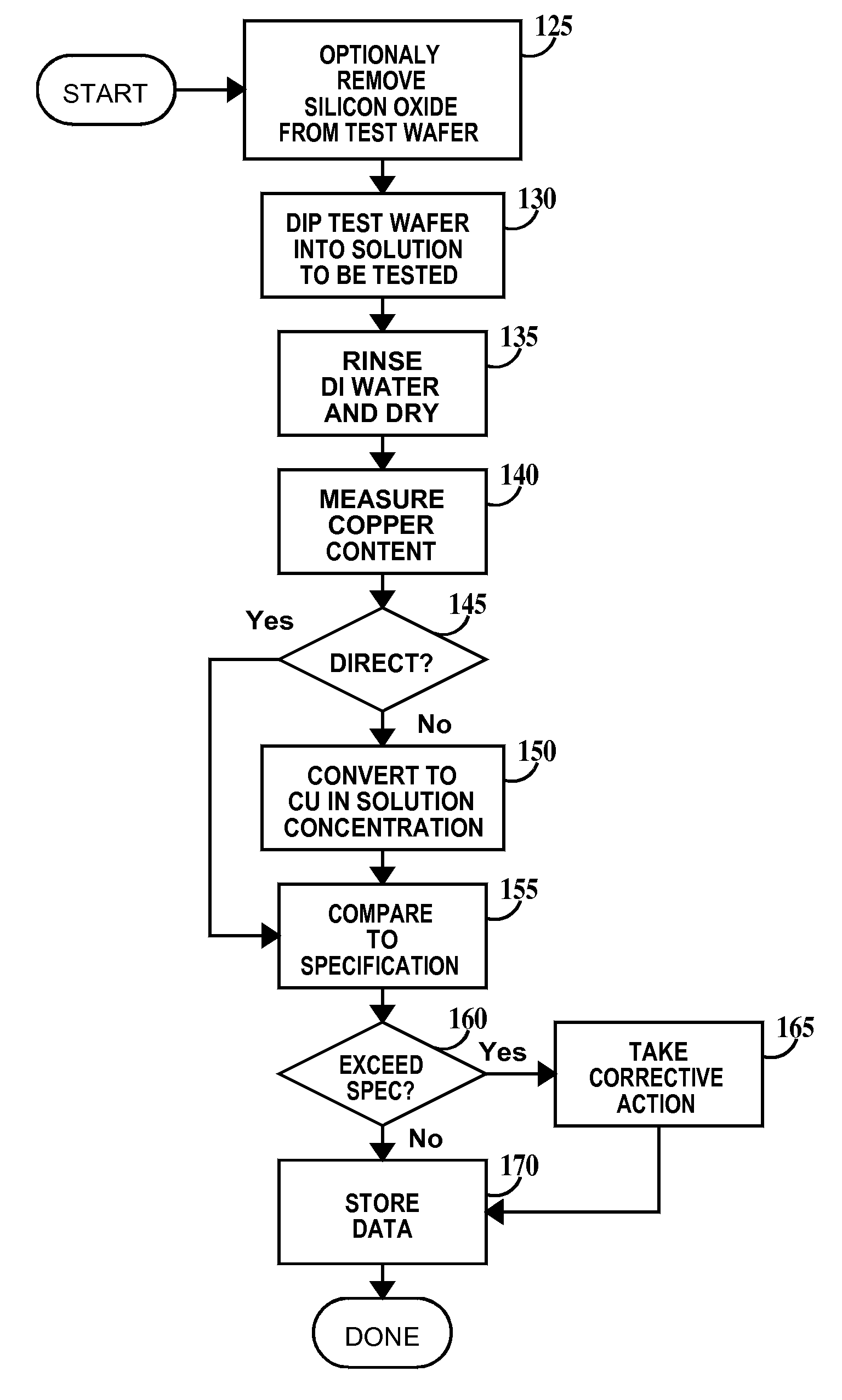
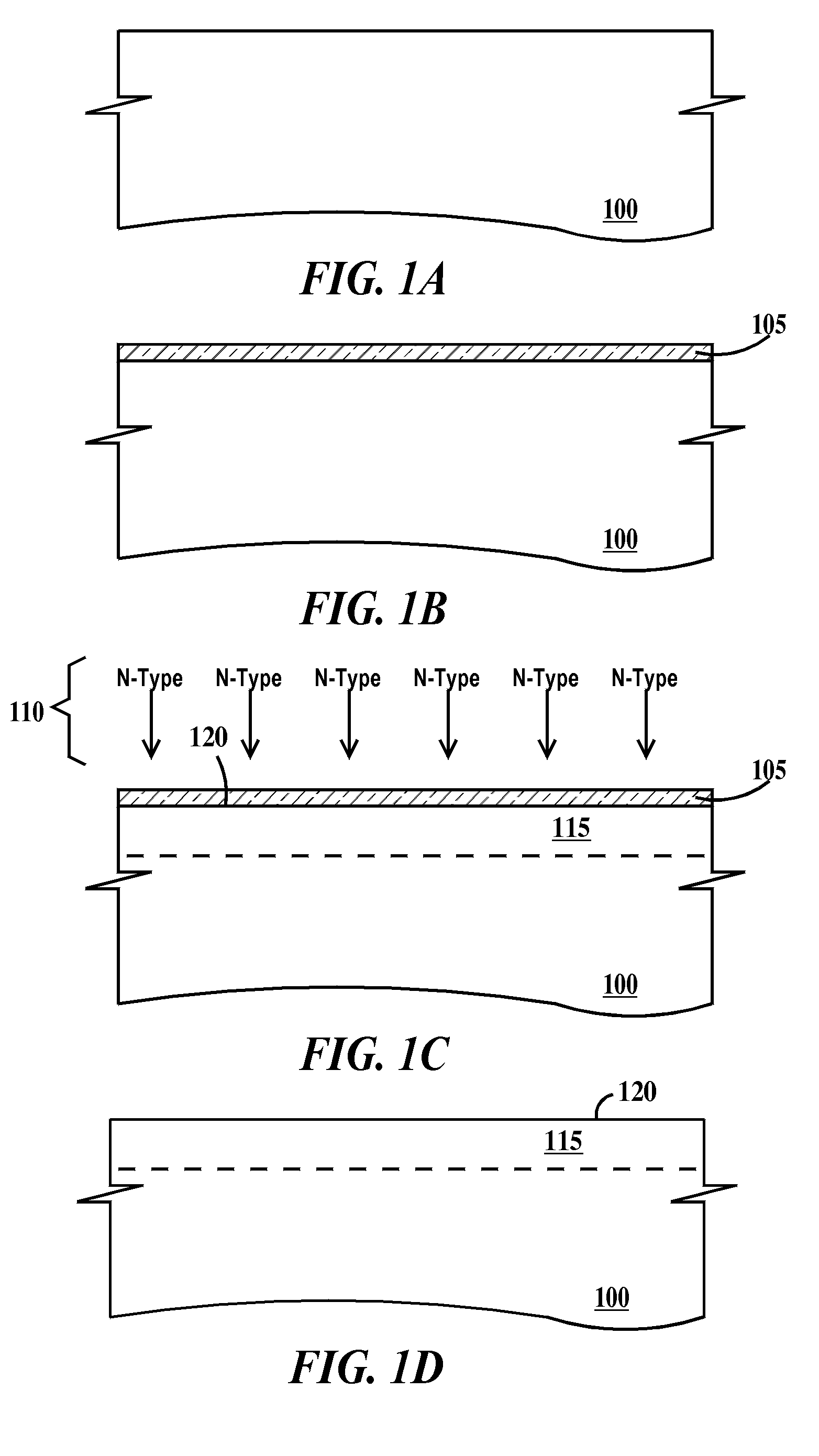
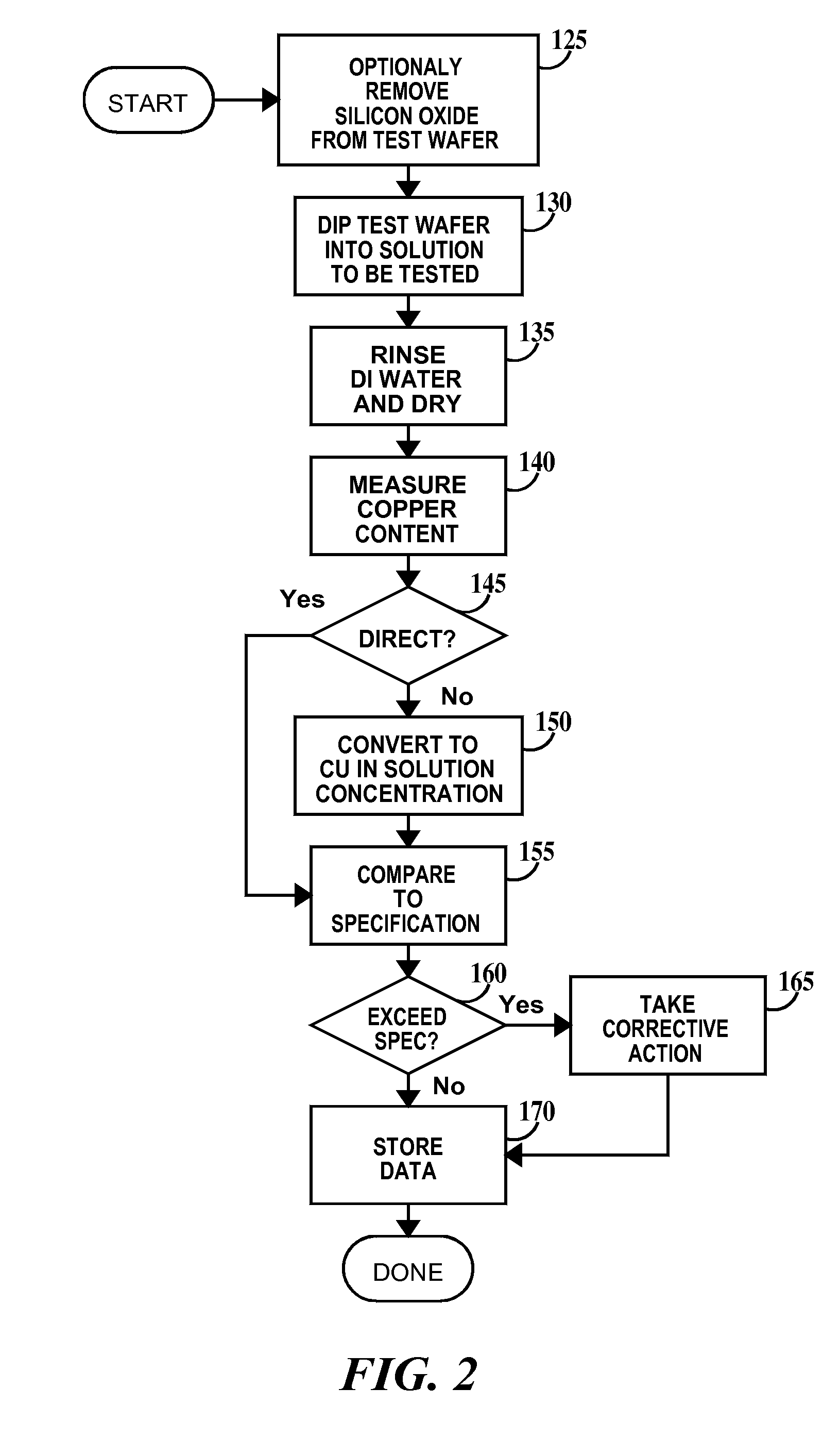
[0027]Integrated circuits are fabricated in silicon layers of disc shaped semiconductor substrates often referred to as wafers. These wafers can have diameters of, to give a few examples, of 125 mm, 200 mm and 300 mm. The fabrication of integrated circuits requires frequent dipping of wafers into tanks containing various neutral, acidic (e.g., hydrofluoric, nitric, sulfuric, phosphoric and acetic) and basic (potassium hydroxide, tetramethylammonium hydroxide, ammonium hydroxide) aqueous wafer cleaning solutions, aqueous wafer etching solutions, aqueous photoresist developing solutions and aqueous photoresist removal solutions. Copper dissolved in these solutions can be adsorbed on the surface of N-type silicon when the surface concentration of N-type dopant (e.g., arsenic, phosphorous) exceeds a threshold value (e.g., about 1 E13 atm / cm2 or higher). The higher the N-type dopant surface concentration, the more copper will be adsorbed on the surface.

[0028]FIGS. 1A through 1D are cross...


PUM


Abstract

A method of monitoring copper contamination. The method includes method, comprising: (a) ion-implanting an N-type dopant into a region of single-crystal silicon substrate, the region abutting a top surface of the substrate; (c) activating the N-type dopant by annealing the substrate at a temperature of 500° C. or higher in an inert atmosphere; (c) submerging, for a present duration of time, the substrate into an aqueous solution, the aqueous solution to be monitored for copper contamination; and (d) determining an amount of copper adsorbed from the aqueous solution by the region of the substrate.

Description

RELATED APPLICATIONS[0001]This application is related to Application Docket No. BUR920070125US2 filed on Sep. 28, 2007.FIELD OF THE INVENTION[0002]The present invention relates to the field of integrated circuit fabrication; more specifically, it relates to a method for monitoring copper contamination in an integrated circuit fabrication facility and a system for monitoring copper contamination in an integrated circuit fabrication facility.BACKGROUND OF THE INVENTION[0003]Modern integrated circuits are fabricated with copper interconnection wiring. Wet processing tanks in the integrated circuit fabrication can be contaminated with copper, causing yield loss and reliability concerns. Accordingly, there exists a need in the art for methods and systems for monitoring copper contamination of solution in wet processing tanks in integrated circuit manufacturing facilities.SUMMARY OF THE INVENTION[0004]A first aspect of the present invention is a method, comprising: (a) ion-implanting an N...

Claims


Application Information

Patent Timeline
IPC IPC(8): H01L21/66
CPCH01L22/20H01L22/12
Inventor BURNHAM, JAY SANFORDVAUGHN COMEAU, JOSEPH KERRYCRANE, LESLIE PETERELLIOTT, JAMES RANDALLESTES, SCOTT ALANNAKOS, JAMES SPIROSWHITE, ERIC JEFFREY
Owner GLOBALFOUNDRIES INC
Why Eureka
Try Eureka