ESD avoiding circuits based on the ESD detectors in a feedback loop

Inactive Publication Date: 2009-04-09
EMEMORY TECH INC
View PDF19 Cites 32 Cited by
  • Summary
  • Abstract
  • Description
  • Claims
  • Application Information

AI Technical Summary

Benefits of technology

[0009]In accordance with an embodiment of the present invention, an ESD avoiding circuit for avoiding passing an electrostatic discharge voltage induced on a connection pad to an internal circuit. The ESD avoiding circuit comprises a first transistor and an ESD detector. The ESD detector comprises a second transistor, a third transistor, and a fourth transistor. The first transistor has a source coupled to the connection pad, a drain coupled to the internal circuit, a gate, and a channel well. The ESD detector is coupled to the first transistor for providing a control signal to the gate of the first transistor. The second transistor has a source coupled to the connection pad, a channel well coupled to the source, a gate coupled to the internal circuit, and a drain coupled to the gate of the first transistor. The third transistor has a source coupled to a ground terminal, a channel well coupled to the source, a gate coupled to the internal circuit, and a drain coupled to the gate of the first transistor. The fourth transistor has a source coupled to the ground terminal, a channel well coupled to the source, a gate coupled to a power terminal, and a drain coupled to the gate of the first transistor.
[0010]The present invention further provides an ESD protection circuit for protecting an i

Problems solved by technology

However, these advanced process technologies also significantly sacrifice the electrostatic discharge (ESD) robustness of the integrated circuit.
Therefore, the ESD is more likely to become a bottleneck in the mass production yield rate of integrated circuits.
However, when the amount of charges being acc

Method used


Image

  • ESD avoiding circuits based on the ESD detectors in a feedback loop
  • ESD avoiding circuits based on the ESD detectors in a feedback loop
  • ESD avoiding circuits based on the ESD detectors in a feedback loop

Examples


first embodiment

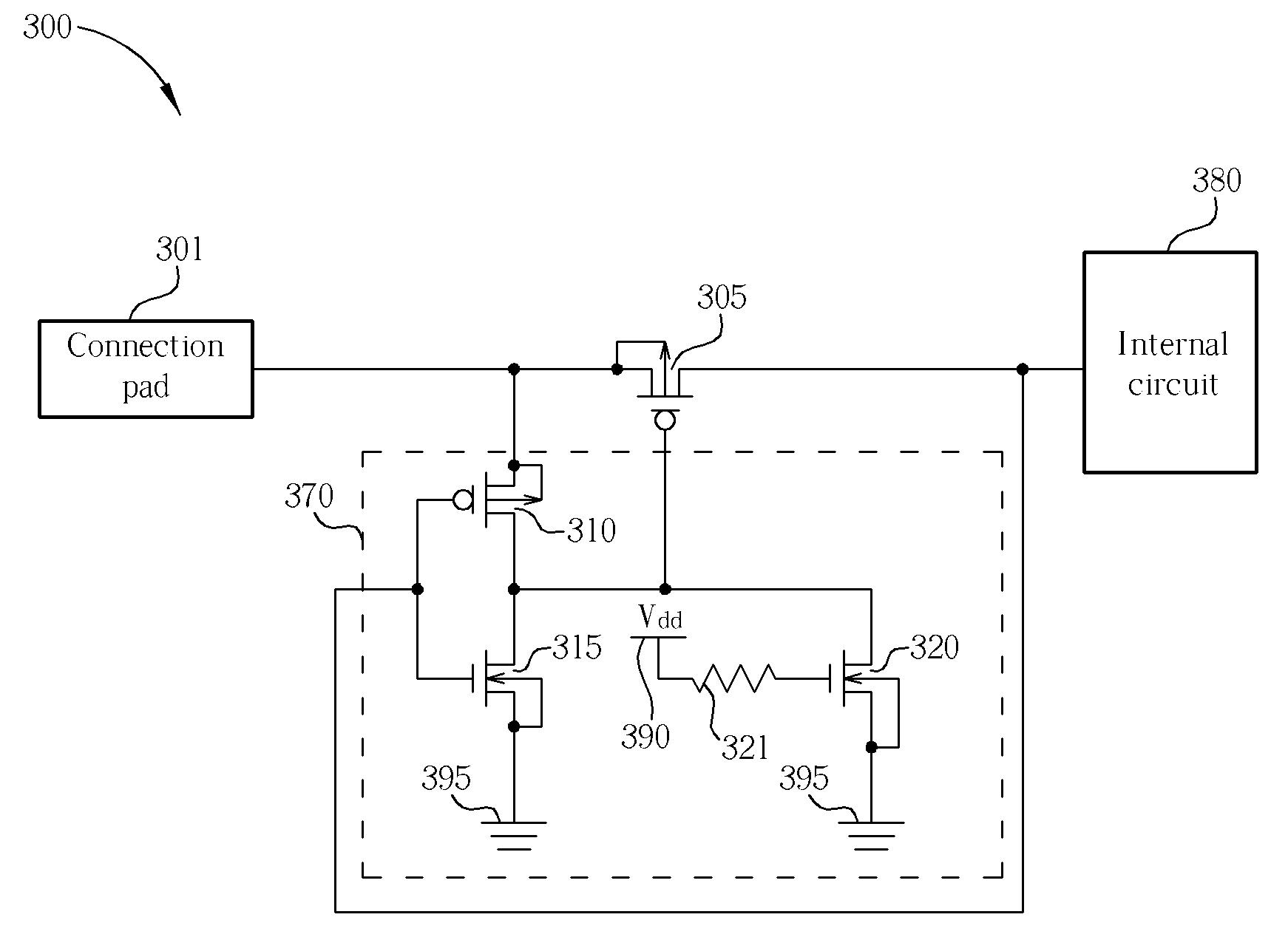
[0021]Please refer to FIG. 3, which is a schematic circuit diagram showing the structure of an ESD avoiding circuit in an integrated circuit 300 in accordance with the present invention. The integrated circuit 300 comprises a connection pad 301, a first transistor 305, an ESD detector 370 and an internal circuit 380. The ESD avoiding circuit in FIG. 3 comprises the first transistor 305 and the ESD detector 370. The ESD detector 370 comprises a second transistor 310, a third transistor 315, a fourth transistor 320 and a resistor 321.

[0022]The first transistor 305 has a source coupled to the connection pad 301, a drain coupled to the internal circuit 380, a gate coupled to the ESD detector 370, and a channel well. The channel well of the first transistor 305 can be coupled to the source of the first transistor 305 or a power terminal 390. The first transistor 305 is a PMOS transistor, and the channel well of the first transistor 305 is an N-type doped well. The ESD detector 370 is cap...

second embodiment

[0030]Please refer to FIG. 4, which is a schematic circuit diagram showing the structure of an ESD avoiding circuit in an integrated circuit 400 in accordance with the present invention. The integrated circuit 400 comprises a connection pad 301, a first transistor 305, an ESD detector 370, a fifth transistor 425, a resistor 426 and an internal circuit 380. The ESD avoiding circuit in FIG. 4 comprises the first transistor 305, the fifth transistor 425, the resistor 426 and the ESD detector 370. The ESD detector 370 comprises a second transistor 310, a third transistor 315, a fourth transistor 320 and a resistor 321. The first transistor 305 has a source coupled to the connection pad 301, a drain coupled to the internal circuit 380, a gate coupled to the ESD detector 370, and a channel well coupled to the power terminal 390.

[0031]The fifth transistor 425 has a source coupled to the connection pad 301, a drain coupled to the internal circuit 380, a gate coupled to resistor 426, and a c...


PUM


Abstract

When an electrostatic discharge event occurs to a connection pad of a chip, an electrostatic discharge detector layout in a feedback loop is able to detect an induced electrostatic discharge voltage for generating a control signal. A pass transistor can be turned off by the control signal for isolating the induced electrostatic discharge voltage, and the internal circuit of the chip can be protected from being damaged by the induced electrostatic discharge voltage. Furthermore, the designed circuit based on electrostatic discharge isolation technique for protecting the internal circuit of the chip is compatible with programmable circuits, and the connection pad can be furnished with burning signals or logic signals.

Description

BACKGROUND OF THE INVENTION [0001]1. Field of the Invention[0002]The present invention relates in general to ESD avoiding circuits, and more particularly, to the ESD avoiding circuits based on the ESD detectors in a feedback loop.[0003]2. Description of the Prior Art[0004]Since the complementary metal-oxide semiconductor (CMOS) production technology has advanced well into the deep-submicron and nanometer scale, integrated circuit (IC) performance has risen correspondingly. Nowadays, many integrated circuits are guided into mass production by the CMOS process. Some advanced process technologies for scaling-down device areas within integrated circuits, such as thinner gate-oxide and shallower drain / source, can effectively increase the integration and improve the characteristics of the devices. However, these advanced process technologies also significantly sacrifice the electrostatic discharge (ESD) robustness of the integrated circuit. Therefore, the ESD is more likely to become a bo...

Claims


Application Information

Patent Timeline
IPC IPC(8): H02H9/04H02H1/00
CPCH02H9/046
Inventor HUANG, SHAO-CHANGSHEN, CHIUN-CHICHEN, HSIN-MING
Owner EMEMORY TECH INC
Why Eureka
Try Eureka