Recording modulation circuit, recording modulation method and optical disk apparatus

a recording modulation and optical disk technology, applied in the field of recording modulation circuit, recording modulation method and optical disk apparatus, can solve the problems of normal reproduction becoming difficult, erroneous data not being recorded on the disk, etc., and achieve the effect of speeding up the recording process, and reducing the creation time of the recording disk

Inactive Publication Date: 2009-04-09
RENESAS ELECTRONICS CORP
View PDF8 Cites 3 Cited by
  • Summary
  • Abstract
  • Description
  • Claims
  • Application Information

AI Technical Summary

Benefits of technology

[0015]In recent years, the DVD disk is operated at 20 times speed faster than 16 times speed which is considered as the limit of the DVD disk so as to use up to the performance limit of the circuit and the drive. As the speed becomes higher, the recording time can be shortened, and the recording disk creation time of the user can be reduced. For instance, in the case of the data requiring 60 minutes when recorded at normal (1×) speed, only 3 minutes are required if the data is recorded at 20 times speed. Such an improvement in recording speed has been strongly desired by the user not only for data but also in high-speed dubbing in the DVD recorder.
[0016]However, as described above, high-speed recording is difficult if the transfer error is output even only once. Further, the memory controller process becomes stricter as the recording speed is increased, and the possibility of causing sporadic and incidental transfer error due to unexpected factors is also increased.
[0017]Therefore, an object of the present invention is to provide an optical disk apparatus and a recording modulation circuit thereof capable of achieving the high-speed recording even if sporadic and incidental transfer error occurs at the time of data input from the memory to the recording modulation circuit, and providing margin to the memory process. In particular, an object of the present invention is to achieve the high-speed recording in the streaming recording in which images are directly recorded on the optical disk.

Problems solved by technology

As described in patent document 2, since the error correction is performed in units of ECC block in reproducing the disk, the data recorded on the disk needs to be continuous data, and normal reproduction becomes difficult if the data is lost or the data order is moved up.
On the other hand, as the cause of interrupting the recording in the circuit, when the transfer data from the memory controller to the recording modulation circuit is delayed for the recording clock, transfer error is output to interrupt the recording operation so that erroneous data is not recorded on the disk.

Method used


Image

  • Recording modulation circuit, recording modulation method and optical disk apparatus
  • Recording modulation circuit, recording modulation method and optical disk apparatus
  • Recording modulation circuit, recording modulation method and optical disk apparatus

Examples


first embodiment

[0044]An optical disk apparatus according to a first embodiment of the present invention will be described below.

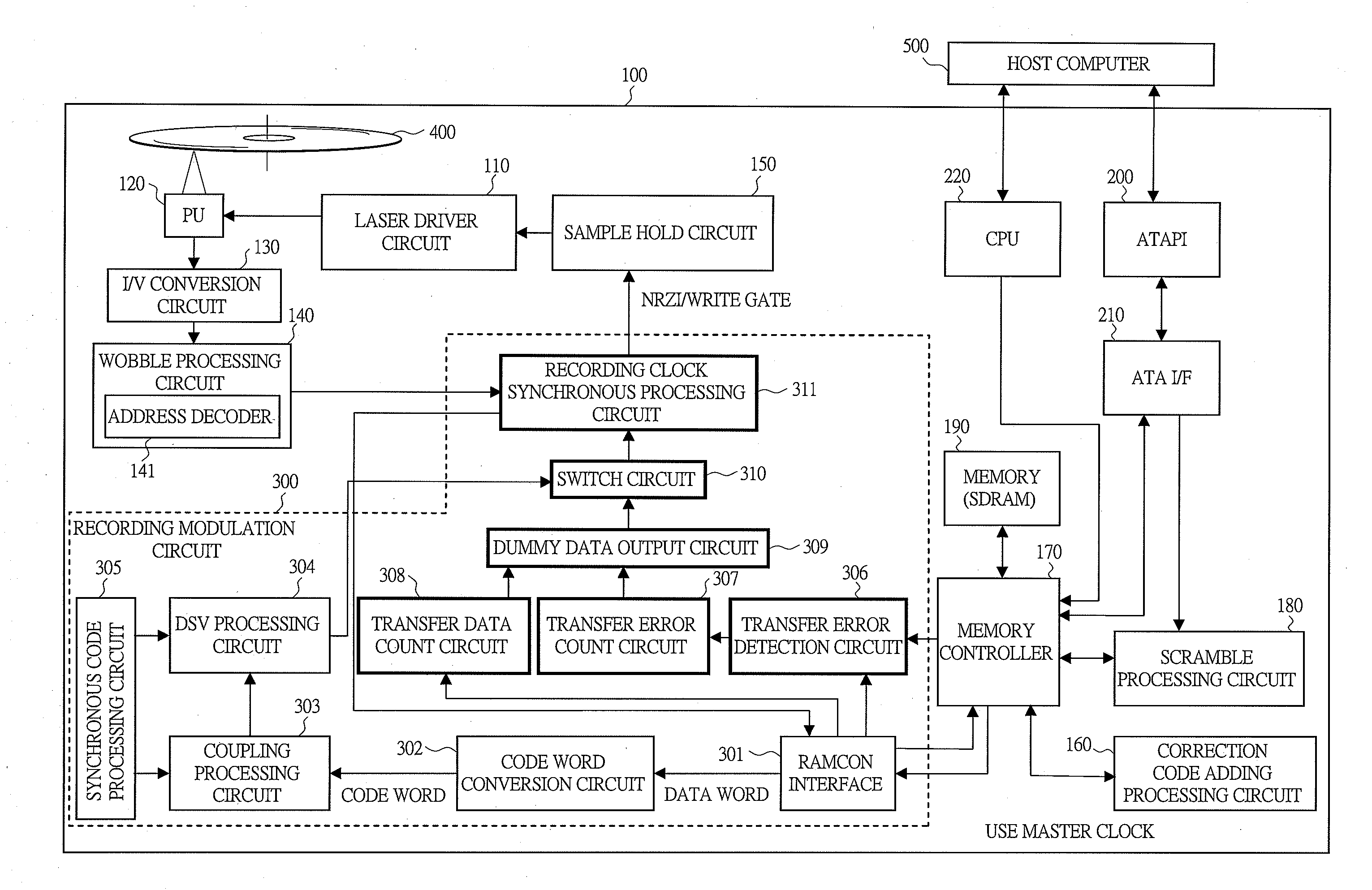
[0045]FIG. 1 is a block diagram of an optical disk apparatus of the present embodiment. In FIG. 1, the optical disk apparatus 100 is configured to include a laser driver circuit 110, an optical head (PU) 120, an I / V conversion circuit 130, a wobble processing circuit 140, a sample hold circuit 150, a correction code adding processing circuit 160, a memory controller 170, a scramble processing circuit 180, a memory 190, an ATAPI 200, an ATAPI interface (ATA I / F) 210, a CPU 220, and a recording modulation circuit 300. Further, the wobble processing circuit 140 includes an address decoder 141.

[0046]Here, the recording modulation circuit 300 is a circuit which performs modulation in accordance with the modulation scheme for modulating a data word of i bits (i is a positive integer) to a code word of j bits (j is a positive integer), and outputs the modulated output data of a ...

second embodiment

[0102]An optical disk apparatus according to the second embodiment will be described below.

[0103]The block diagram of the optical disk apparatus according to the present embodiment is similar to FIG. 1 of the first embodiment. In the optical disk apparatus 100 of the present embodiment, when the number of transfer errors in units of sync frame is larger than the predetermined number of times, the dummy data equivalent to one ECC block is output from the recording modulation circuit 300 to the sample hold circuit 150, and correct data is output from the next ECC block in the memory 190.

[0104]In this case, the correct code word is switched and output from the next ECC block by the data switch circuit 309 at the timing determined by the data count value of the transfer data count circuit 308 that is the number of times of normal data transfer from the memory controller 170 and the transfer error count value of the transfer error count circuit 307.

[0105]FIG. 7 is a view showing the writ...

third embodiment

[0109]An optical disk apparatus according to a third embodiment of the present invention will be described below.

[0110]In the optical disk apparatuses of the first embodiment and the second embodiment, the dummy data is output without dropping the write gate at the point where the transfer error is detected. On the other hand, in the optical disk apparatus 100 of the present embodiment, the write gate is dropped at the point where the transfer error is detected, whereby the NRZI is not output from the recording modulation circuit 300 and the recording is not performed.

[0111]FIG. 8 is a view showing the write gate and the NRZI of the present embodiment. At the point where the transfer error is detected in the transfer error detection circuit 306, the write gate output from the recording clock synchronous processing circuit 311 is dropped, whereby the NRZI is not output and recording is not performed. Thereafter, if the transfer error is not output, the write gate may be raised at the...


PUM

PropertyMeasurementUnit
lengthaaaaaaaaaa
lengthaaaaaaaaaa
lengthaaaaaaaaaa

Abstract

After a transfer error detection circuit detects a transfer error that transfer data from a memory controller to a recording modulation circuit is delayed for a recording clock process, the number of transfer errors is counted in units of sync frame in a transfer error count circuit. When the number of transfer errors is n times (n: positive integer) or less, the modulation and recording operation are continued as it is and the NRZI output operation is performed from the correct position while applying a sync, and when the number of transfer errors is n times or larger, the recording operation is interrupted and the re-recording is performed from the interrupted location thereafter.

Description

CROSS-REFERENCE TO RELATED APPLICATION[0001]The present application claims priority from Japanese Patent Application No. JP 2007-261701 filed on Oct. 5, 2007 and Japanese Patent Application No. JP 2008-214549 filed on Aug. 22, 2008, the contents of which are hereby incorporated by reference into this application.TECHNICAL FIELD OF THE INVENTION[0002]The present invention relates to a technology effectively applied to a recording modulation circuit and a recording modulation method used in recording digital data on an optical disk and an optical disk apparatus provided with the recording modulation circuit.BACKGROUND OF THE INVENTION[0003]Japanese Patent Application Laid-Open Publication No. 2003-59184 ((FIG. 1 to FIGS. 5A and 5B) patent document 1) discloses a method in which the amount of positional shift is detected and a sync width included in the recorded data is controlled in accordance with the detected amount in order to re-record on a recordable optical disk media such as DV...

Claims


Application Information

Patent Timeline
Patent Type & Authority Applications(United States)
IPC IPC(8): G11B20/18
CPCG11B20/1833G11B2020/1288G11B2220/2579G11B2020/1823G11B2220/2541G11B2020/1453
Inventor MOCHIZUKI, MISUZUNISHIMURA, KOICHIRO
Owner RENESAS ELECTRONICS CORP
Why Eureka
Try Eureka