A/D converter, digital PLL circuit using the same, and information recording apparatus using the same
a converter and digital technology, applied in the field of a/d converters, digital pll circuits, information recording apparatuses, can solve the problems of difficult to reduce the difference between lsis and high-speed a/d converters with a large circuit scale, and achieve the effect of high phase precision and suitable for lsi integration
- Summary
- Abstract
- Description
- Claims
- Application Information
AI Technical Summary
Benefits of technology
Problems solved by technology
Method used
Image
Examples
first embodiment
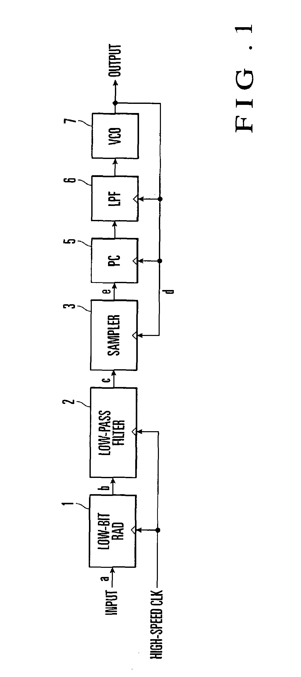
[0024]As shown in FIG. 1, a digital PLL circuit according to the first embodiment comprises a low-bit resolution A / D (low-bit RAD) 1, low-pass digital filter 2, sampler 3, digital phase comparator 5, digital loop filter 6, and digital VCO 7 which are series-connected to each other. The low-bit resolution A / D 1 receives a signal, and the digital VCO 7 outputs a clock. The low-bit resolution A / D 1 and low-pass digital filter 2 receive a high-speed clock. The sampler 3, digital phase comparator 5, and digital loop filter 6 receive a clock (digital PLL output) output from the digital VCO 7.
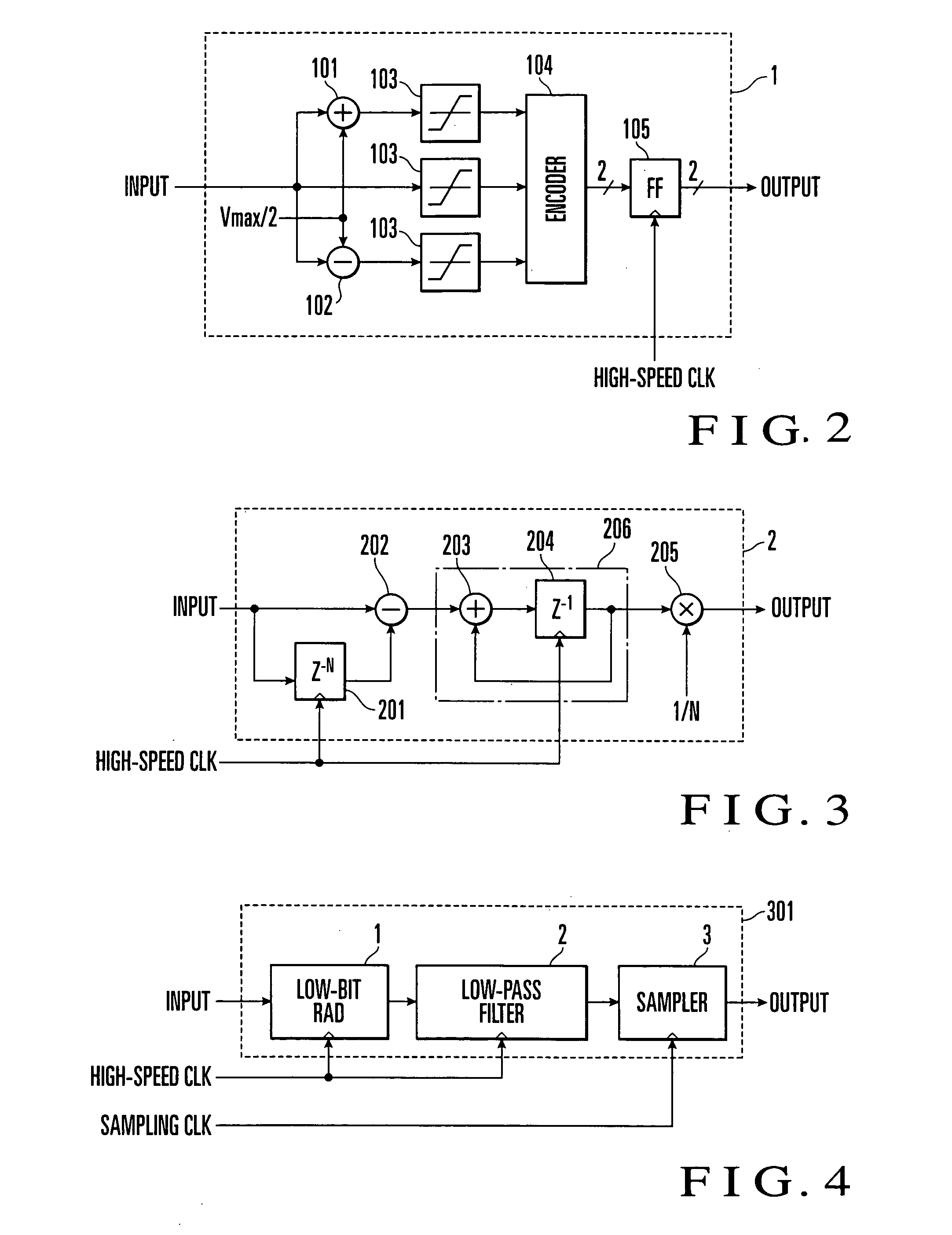
[0025]A signal input to the low-bit resolution A / D 1 may be a signal on which noise is superposed, or an SIN-wave signal. The low-bit resolution A / D 1 may be configured to encode slicer results of different threshold levels. FIG. 2 shows an example of the 2-bit low-bit resolution A / D 1 formed from three slicers. In the low-bit resolution A / D 1 shown in FIG. 2, an input signal is input to slicers 103 d...
second embodiment
[0038]An A / D converter according to the second embodiment of the present invention will be described with reference to FIG. 4. Referring to FIG. 4, an A / D converter 301 in a broad sense comprises an low-bit resolution A / D 1, low-pass digital filter 2, and sampler 3. A high-speed CLK which regulates the operations of the low-bit resolution A / D 1 and low-pass digital filter 2 is set much higher than the sampling CLK of the sampler 3. Compared to a general A / D converter, the A / D converter 301 exhibits a low precision of amplitude information at a portion other than a portion near the edge, but can be utilized as an A / D converter for demodulating, e.g., a frequency- or phase-modulated signal.
third embodiment
[0039]An optical disk information recording apparatus according to the third embodiment of the present invention will be described with reference to FIG. 5. Wobble information is superposed on a push-pull signal read from by an optical head 13 from an optical disk 14 having a guide groove wobbled at a frequency untrackable by the tracking actuator of the optical head 13. An A / D converter 301 formed from a conversion circuit 1, low-pass digital filter 2, and sampler 3 extracts, from the signal, phase information of the wobble signal as digital information. The band of the digital information is limited by a band-pass digital filter 4, and then phase error information is generated by a digital phase comparator 5. A control signal corresponding to the phase error information generated by the digital phase comparator 5 is generated by a digital loop filter 6. The control signal corrects frequency information for a digital VCO 7.
[0040]The output clock frequency of the digital VCO 7 is co...
PUM
| Property | Measurement | Unit |
|---|---|---|
| wobble frequency | aaaaa | aaaaa |
| frequency | aaaaa | aaaaa |
| cutoff frequency | aaaaa | aaaaa |
Abstract
Description
Claims
Application Information


