Nonvolatile Semiconductor Memory Device

Inactive Publication Date: 2009-04-16
SHARP KK
View PDF15 Cites 39 Cited by
  • Summary
  • Abstract
  • Description
  • Claims
  • Application Information

AI Technical Summary

Benefits of technology

[0034]According to the nonvolatile semiconductor memory device having the eleventh characteristics, when the word line or the bit line is formed of a high melting point metal material, polycrystalline silicon, or a compound of the high melting point metal material and polycrystalline silicon, although the wiring resistance thereof is h

Problems solved by technology

Unfortunately, according to the nonvolatile semiconductor memory device at present, memory cells are arranged on a monocrystalline silicon substrate two-dimensionally in general, and confined to a tw

Method used


Image

  • Nonvolatile Semiconductor Memory Device
  • Nonvolatile Semiconductor Memory Device
  • Nonvolatile Semiconductor Memory Device

Examples


Embodiment Construction

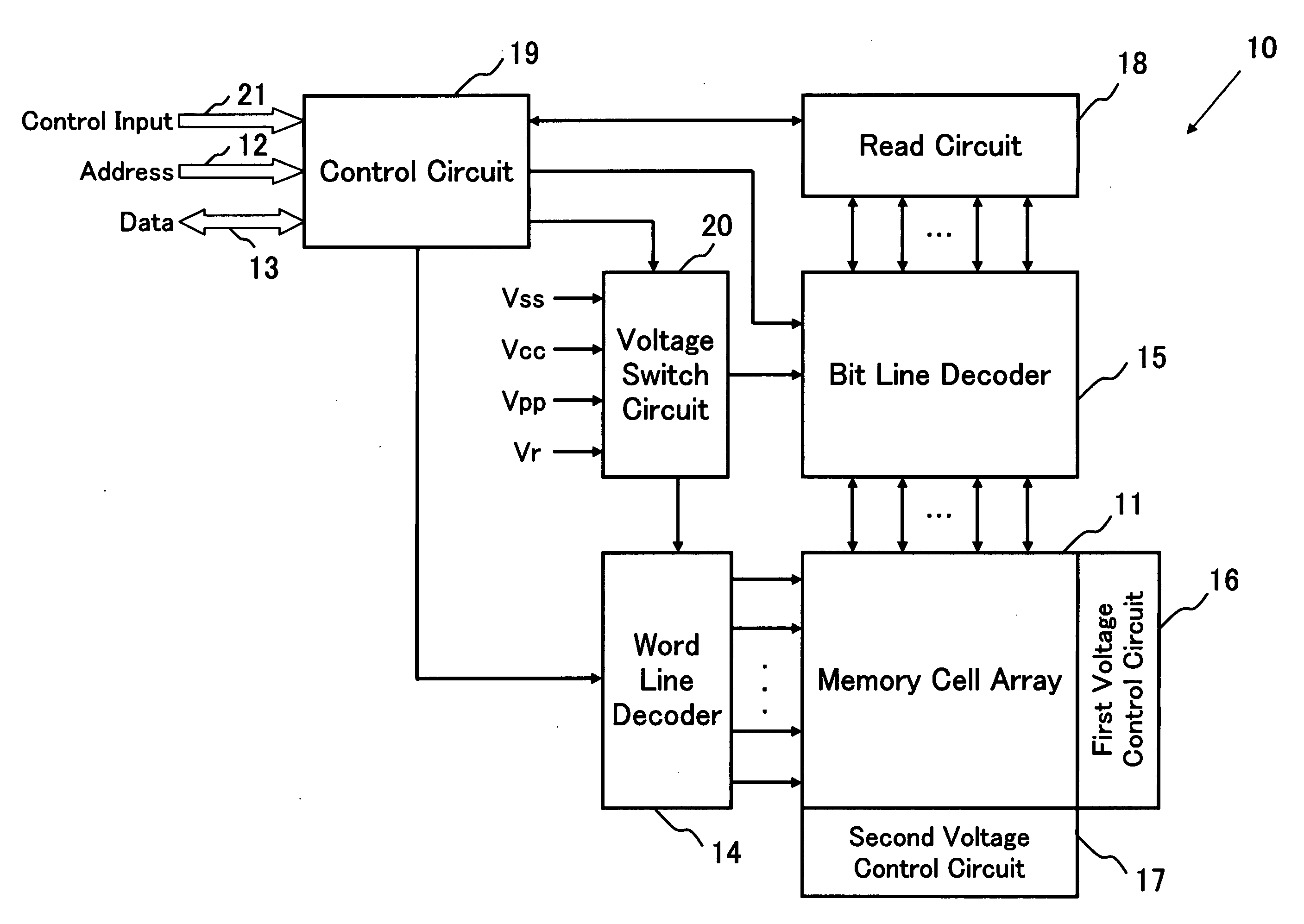
[0078]A nonvolatile semiconductor memory device according to the present invention (referred to as “device of the present invention” for short occasionally hereinafter) will be described with reference to the drawings hereinafter.

[0079]FIG. 1 is a block diagram showing one embodiment of a device 10 of the present invention. As shown in FIG. 1, the device 10 of the present invention includes a memory cell array 11, a word line decoder (corresponding to a word line selection circuit) 14, a bit line decoder (corresponding to a bit line selection circuit) 15, a first voltage control circuit (corresponding to voltage control circuit) 16, a second voltage control circuit (corresponding to a voltage control circuit) 17, a read circuit 18, a control circuit 19, and a voltage switch circuit 20.

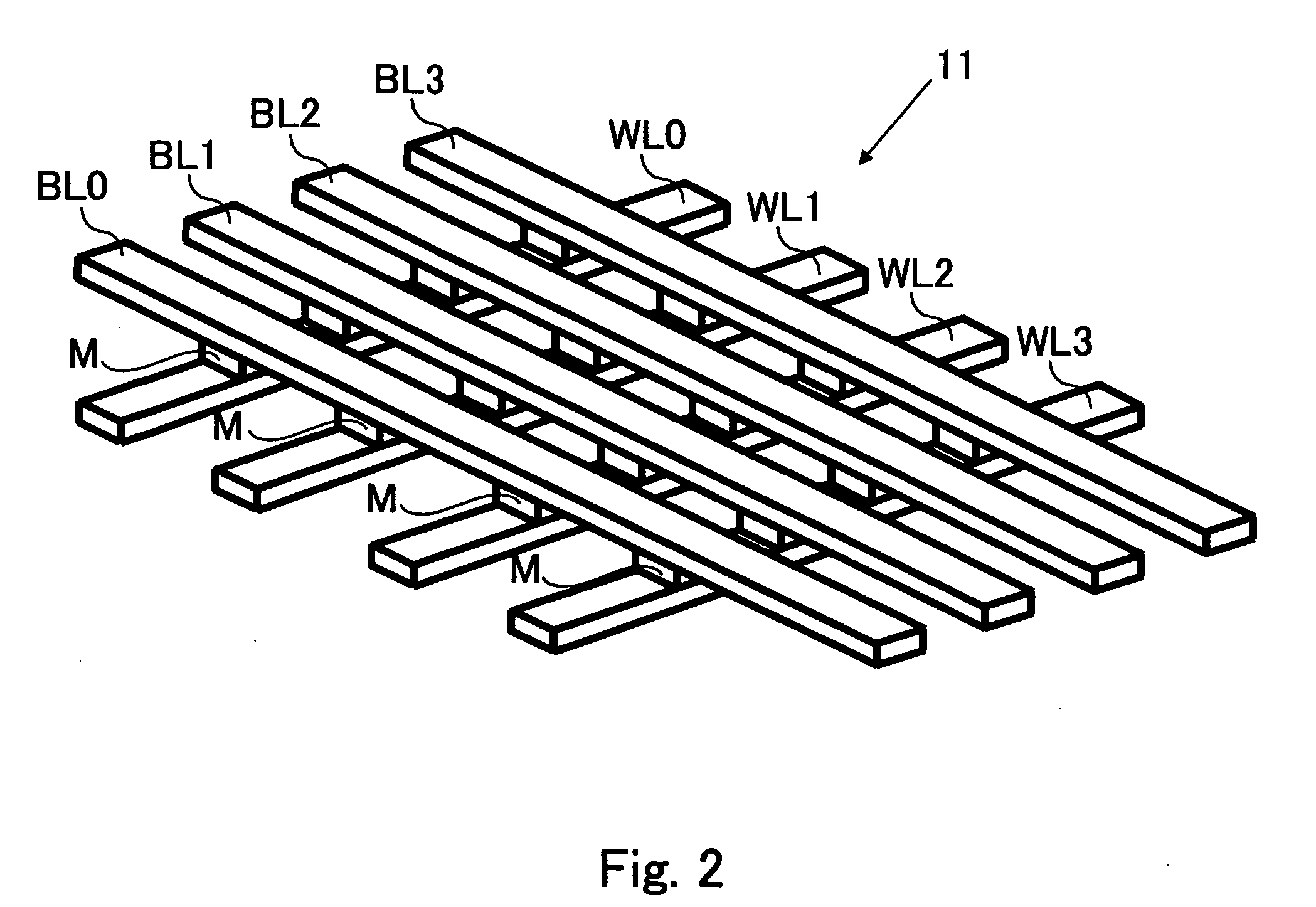
[0080]The memory cell array 11 includes a plurality of nonvolatile memory cells arranged in row and column directions, and information can be programmed electrically in the memory cell specified by an ...


PUM


Abstract

A nonvolatile semiconductor memory device can prevent memory characteristics from deteriorating due to IR drop on word or bit lines in a cross-point type memory cell array. The device comprises a word line selection circuit selecting a selected word line from word lines and applying selected and unselected word line voltages to the selected and unselected word lines, respectively, a bit line selection circuit selecting a selected bit line from bit lines and applying selected and unselected bit line voltages to the selected and unselected bit lines, respectively, and voltage control circuits preventing voltage fluctuation of at least either one of the word and bit lines, wherein at least either one of the word and bit lines are connected to the voltage control circuits at a voltage control point positioned at a farthest point from a drive point connected to the word line selection circuit or bit line selection circuit.

Description

CROSS-REFERENCE TO RELATED APPLICATIONS[0001]This application is a National Phase filing under 35 U.S.C. § 371 of International Application No. PCT / JP2006 / 321817 filed on Nov. 1, 2006, and which claims priority to Japanese Patent Application No. 2005-362646 filed on Dec. 16, 2005.TECHNICAL FIELD[0002]The present invention relates to a nonvolatile semiconductor memory device having a cross-point type memory cell array in which a plurality of two-terminal structured memory cells are disposed in a row direction and a column direction, a plurality of word lines extend in the row direction, a plurality of bit lines extend in the column direction, one ends of the memory cells connected to the same row are connected to the common word line, and the other ends thereof connected to the same column are connected to the common bit line.BACKGROUND ART[0003]As an integrated circuit and the function of a computer are improved, a new application requiring a function for storing large amount of dat...

Claims


Application Information

Patent Timeline
IPC IPC(8): G11C5/02G11C11/34G11C11/00G11C7/00
CPCG11C13/0004G11C13/0007G11C13/004G11C13/0069G11C2213/77G11C2013/009G11C2213/31G11C2213/32G11C2213/34G11C17/18
Inventor MORIMOTO, HIDENORI
Owner SHARP KK
Why Eureka
Try Eureka