

Method of producing semiconductor device
a technology of semiconductor devices and semiconductor layers, applied in semiconductor devices, semiconductor/solid-state device details, electrical devices, etc., can solve the problems of epitaxial layer defects and -type semiconductors, and achieve the effects of reducing the stress of the mask, and improving the efficiency of the production process
- Summary
- Abstract
- Description
- Claims
- Application Information
AI Technical Summary
Benefits of technology
Problems solved by technology
Method used
Image

Examples
Embodiment Construction
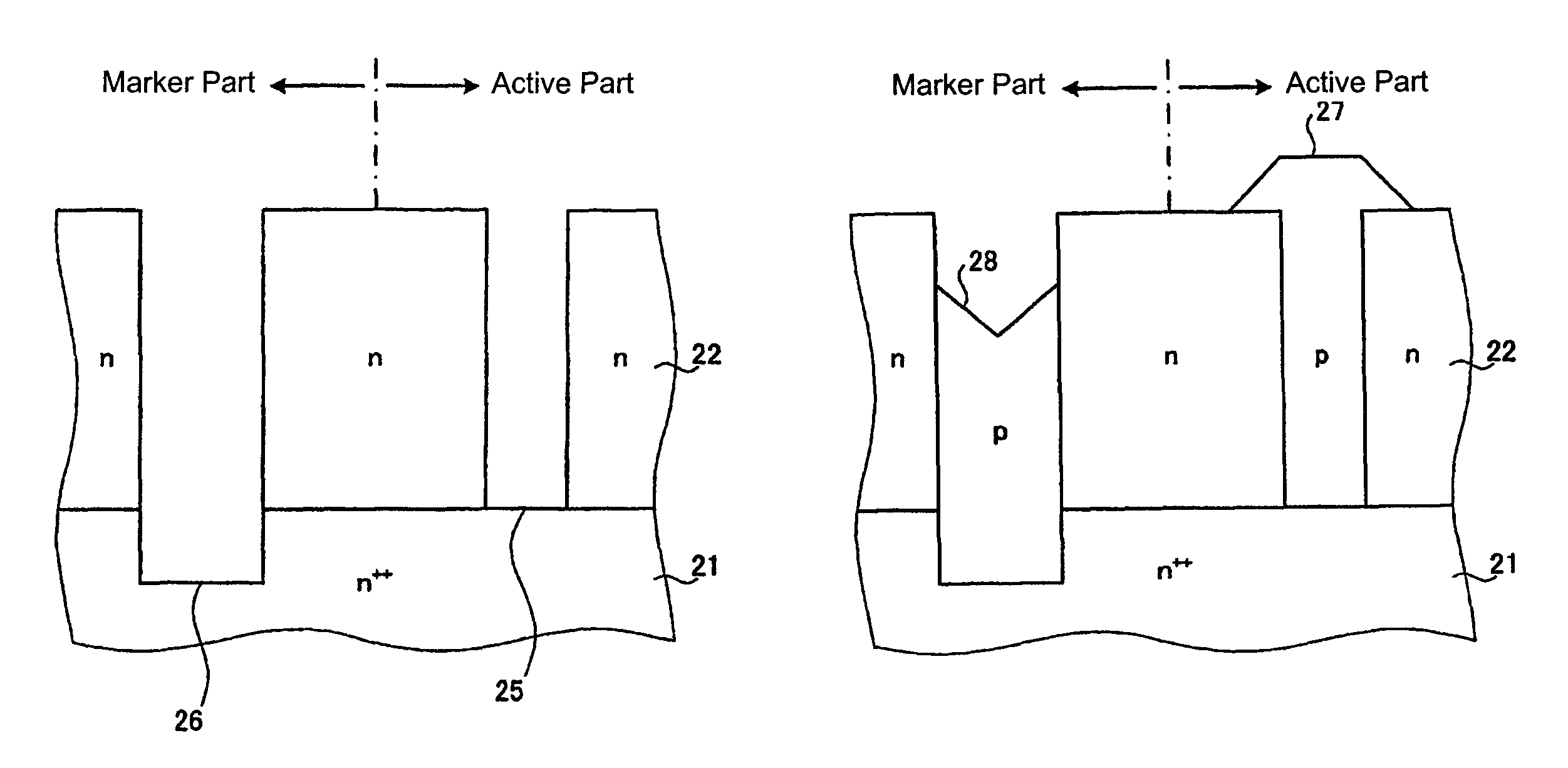
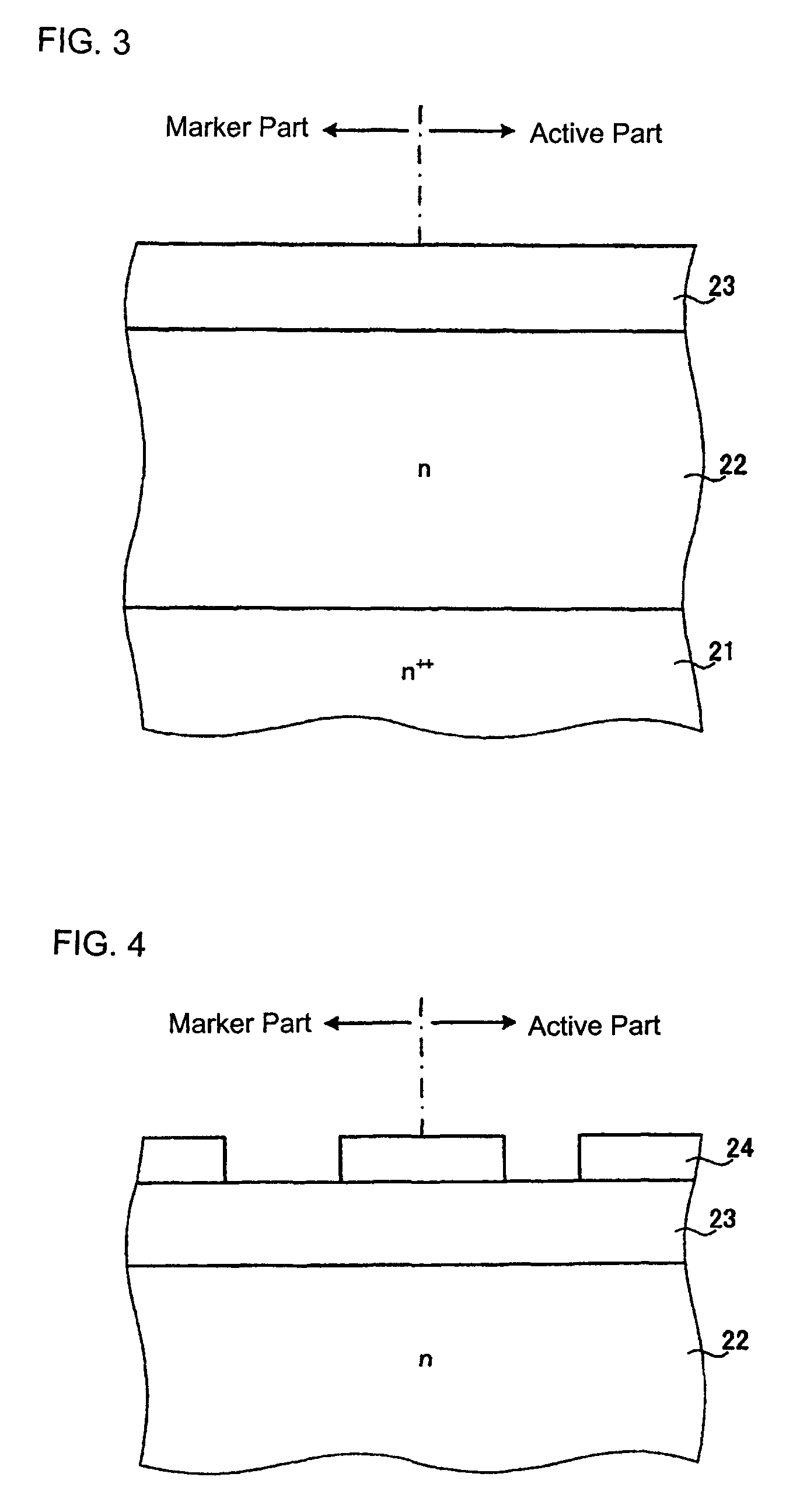
[0026]In this specification and the accompanying drawings, the prefix ‘n’ or ‘p’ attached to a layer or region means that electrons or holes are majority carriers. The superscript ‘+’ attached to the prefix ‘n’ means that the impurity concentration of the layer or region is higher than that of a layer or region having no superscript ‘+’ Incidentally, in the following description of embodiment and the accompanying drawings, like numerals refer to like constituent parts for the sake of avoidance of duplicate description.
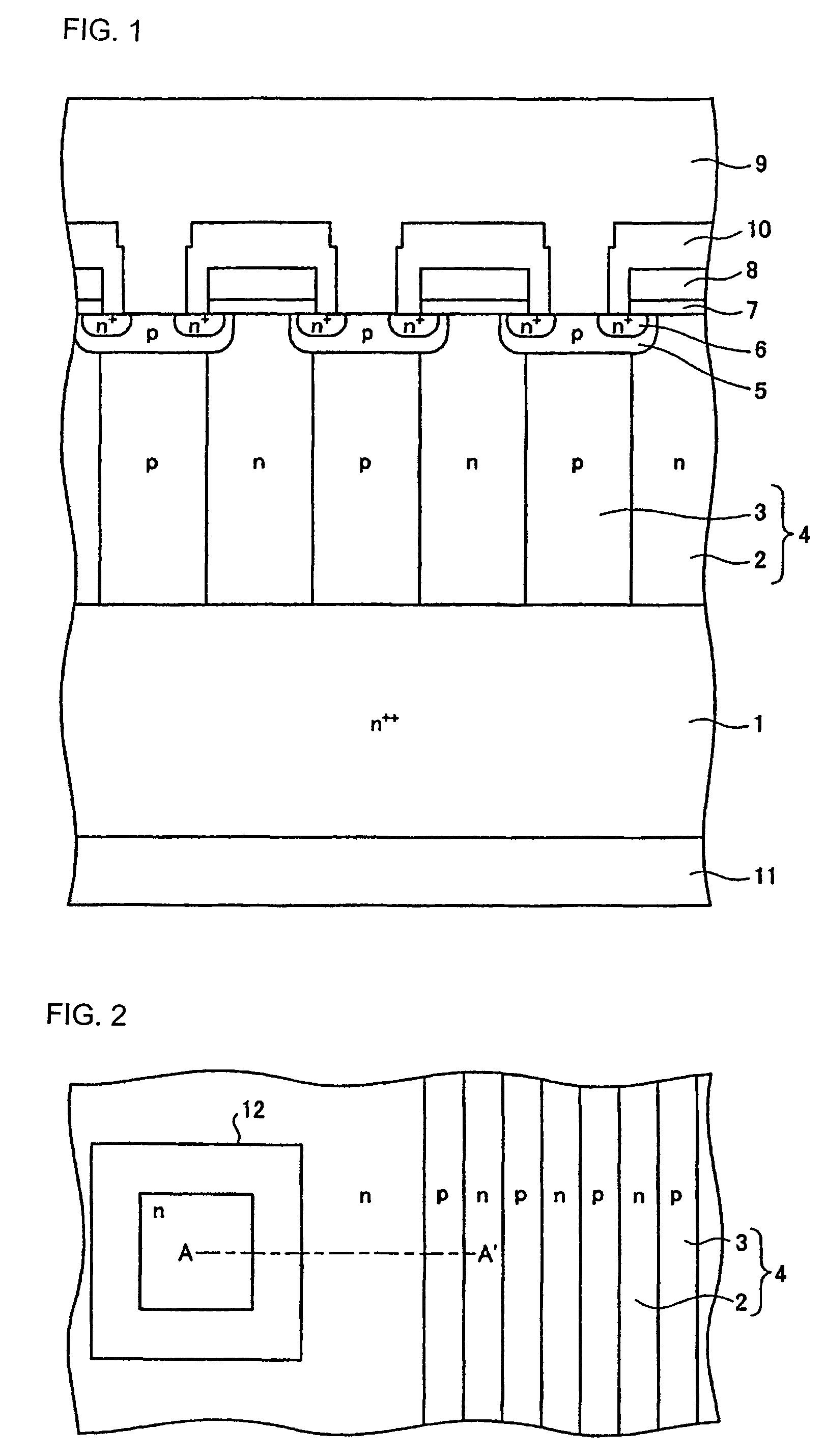
[0027]FIG. 1 is a sectional view showing an example of a super junction semiconductor device produced by a producing method according to the invention. Description will be made in the case where a vertical MOSFET is used as an example. As shown in FIG. 1, a parallel pn structure 4 in which n-type semiconductor regions 2 and p-type semiconductor regions 3 are joined alternately is provided on a low resistance n++ drain layer 1. A high impurity concentration p base regio...
PUM
 Abstract
Description
Claims
Application Information