Method for manufacturing a semiconductor device by exposing, to a hydrogen plasma atmosphere, a semiconductor substrate

a technology of semiconductor devices and substrates, applied in the direction of semiconductor devices, basic electric elements, electrical appliances, etc., can solve problems such as device characteristics that may deteriorate, and achieve the effects of preventing deterioration of device characteristics, excellent ohmic contact, and short tim

Active Publication Date: 2017-05-30
FUJI ELECTRIC CO LTD
View PDF12 Cites 4 Cited by
  • Summary
  • Abstract
  • Description
  • Claims
  • Application Information

AI Technical Summary

Benefits of technology

[0022]According to the aforementioned configurations, after the contact hole has been formed, the transition metal film is formed without inserting a step of forming a metal film (barrier metal) or an oxide film in the surface of the barrier metal in order to prevent hydrogen radicals and hydrogen atoms from penetrating downward. Accordingly, an oxide film in the surface of a silicon carbide semiconductor portion exposed in the contact hole can be removed before the transition metal film is formed. In this manner, the silicon carbide semiconductor portion and the transition metal film can be brought into direct contact with each other. Accordingly, the transition metal film can be silicified by subsequent hydrogen plasma treatment to form an ohmic contact with the silicon carbide semiconductor portion. In addition, the barrier metal or the oxide film in the surface of the barrier metal is formed after the transition metal film has been formed. Accordingly, even when the oxide film on the surface of the silicon carbide semiconductor portion has been removed by cleaning treatment using hydrogen fluoride before the transition metal film is formed, the oxide film in the surface of the barrier metal is not removed. In this manner, even when the barrier metal made of a transition metal has been formed, hydrogen plasma treatment can be performed in the state in which the barrier metal is covered with the oxide film. Accordingly, the barrier metal does not generate heat when the oxide film in the surface of the barrier metal is being reduced. Thus, an extra thermal history is not applied to the portion covered with the barrier metal, i.e. an MOS gate located on the lower side (on the semiconductor substrate side) of the barrier metal. In addition, the barrier metal and the oxide film in the surface of the barrier metal are formed after the transition metal film has been formed. Accordingly, no oxide film is formed in the surface of the transition metal film. Thus, the temperature of only the transition metal film can be increased to a high temperature in a short time.
[0023]According to the method for manufacturing a semiconductor device according to the invention, it is possible to obtain an effect in which an excellent ohmic contact low in contact resistance can be formed and device characteristic can be prevented from deteriorating.

Problems solved by technology

There is a concern that, for example, device characteristic may deteriorate due to a thermal history caused by the heating.

Method used


Image

  • Method for manufacturing a semiconductor device by exposing, to a hydrogen plasma atmosphere, a semiconductor substrate
  • Method for manufacturing a semiconductor device by exposing, to a hydrogen plasma atmosphere, a semiconductor substrate
  • Method for manufacturing a semiconductor device by exposing, to a hydrogen plasma atmosphere, a semiconductor substrate

Examples


embodiment

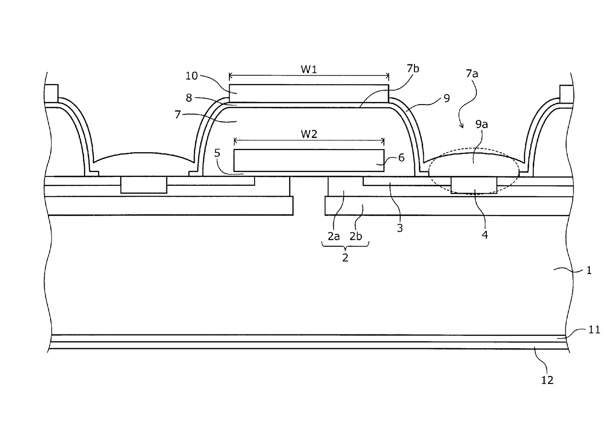
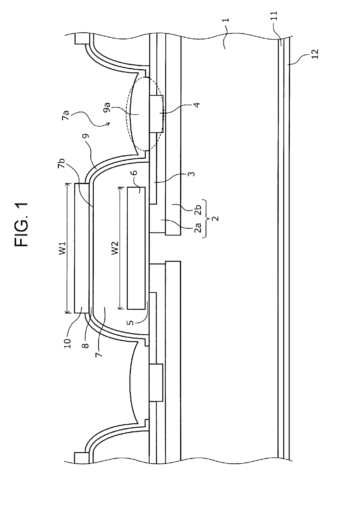
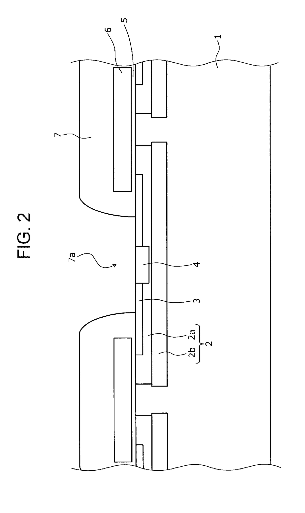
[0034]An MOSFET (Metal Oxide Semiconductor Field Effect Transistor) will be described as an example of a semiconductor device manufactured by a method for manufacturing a semiconductor device according to an embodiment. FIG. 1 is a sectional view showing the structure of an example of a semiconductor device manufactured by the method for manufacturing a semiconductor device according to the embodiment. As shown in FIG. 1, the semiconductor device according to the embodiment is a vertical type MOSFET with a planar gate structure. The vertical type MOSFET is provided with an MOS gate structure and a front surface electrode (source electrode) on a front surface side of a semiconductor substrate made of silicon carbide (silicon carbide substrate (semiconductor chip)), and provided with a back surface electrode (drain electrode 12) on a back surface side of the silicon carbide substrate.

[0035]Specifically, a p-type base region 2 is selectively provided in a surface layer of the front sur...


PUM

PropertyMeasurementUnit
temperatureaaaaaaaaaa
thicknessaaaaaaaaaa
thicknessaaaaaaaaaa

Abstract

A method for manufacturing a semiconductor device having a MOS gate structure includes forming a device structure on a semiconductor substrate; forming an interlayer dielectric to cover the device structure; forming a contact hole through the interlayer dielectric; forming a transition metal film (e.g., Ni) on a portion of the semiconductor substrate exposed by the contact hole; (e) forming a metal film (e.g., Ti) on the entire surface of the semiconductor substrate; forming an oxide film in the surface of the metal film; selectively removing the metal film in which the oxide film has been formed, to thereby expose the transition metal film; and (h) exposing, to a hydrogen plasma atmosphere, the semiconductor substrate in which the transition metal film and the oxide film have been exposed, to thereby cause the transition metal film to generate heat and react with the semiconductor substrate and form an ohmic contact there between.

Description

CROSS-REFERENCE TO RELATED APPLICATION(S)[0001]This non-provisional Application for a U.S. Patent claims priority from JP PA 2014-220810 filed Oct. 29, 2014, the entire contents of which are hereby incorporated by reference.BACKGROUND OF THE INVENTION[0002]1. Field of the Invention[0003]The present invention relates to a method for manufacturing a semiconductor device.[0004]2. Description of the Related Art[0005]According to the background art, it has been well known that an ohmic contact (electric contact portion) between a silicon carbide semiconductor portion and a metal film (electrode) in a semiconductor device (silicon carbide semiconductor device) using a silicon carbide (SiC) semiconductor is formed by thermal treatment (annealing). A method for manufacturing the semiconductor device according to the background art will be described. FIG. 9 is a sectional view schematically showing a state in which the semiconductor device is being manufactured according to the background ar...

Claims


Application Information

Patent Timeline
Patent Type & Authority Patents(United States)
IPC IPC(8): H01L21/3213H01L21/04H01L29/16H01L29/66H01L29/45
CPCH01L29/1608H01L21/0485H01L21/32139H01L29/66068H01L29/45H01L21/02063H01L21/02068H01L29/41741H01L29/401
Inventor OGINO, MASAAKI
Owner FUJI ELECTRIC CO LTD
Why Eureka
Try Eureka