Method for determining a dopant concentration in a semiconductor sample

a semiconductor and concentration technology, applied in the field of semiconductor concentration determination, can solve problems such as periodic lattice distortion, and achieve the effect of small contact radius and higher local resolution

Inactive Publication Date: 2009-04-16
FRAUNHOFER GESELLSCHAFT ZUR FOERDERUNG DER ANGEWANDTEN FORSCHUNG EV
View PDF7 Cites 12 Cited by
  • Summary
  • Abstract
  • Description
  • Claims
  • Application Information

AI Technical Summary

Benefits of technology

[0014]The method, which is designated by the applicant as Scanning Schottky Vibration Spectroscopy (SSVM), differs from the previously known methods in that it uses contact resonances, wherein the oscillations of the lead spring are measured. In this case, the leaf spring tip is a metal or is at least coated with a metal layer and forms a so-called Schottky barrier or Schottky contact on contact with the semiconductor surface, during which, as a result of the different Fermi levels between semiconductor and metal, a space charge zone is created, which is formed as a charge carrier depletion layer in the semiconductor. If an electrical alternating voltage is applied in the region of the Schottky contact, the size of the space charge zone varies depending on the alternating voltage, that is it becomes larger or smaller. The variation in the thickness of the forming space charge zone is associated with a lattice distortion of the semiconductor material which again can have different causes. According to the present understanding of the effect to be observed, in which the semiconductor material exhibits local oscillating volume fluctuations, it is assumed that lattice distortions are formed by means of the attraction between the negative electrons in the metal and positively charged atomic cores in the electron depletion zone in the semiconductor. The periodic lattice distortions in the doped region bring about periodic lattice distortions in the surrounding semiconductor sample and can likewise excite the leaf spring in c...

Problems solved by technology

The periodic lattice distortions in the doped region bring about periodic lattice distortions in the surrounding s...

Method used


Image

  • Method for determining a dopant concentration in a semiconductor sample
  • Method for determining a dopant concentration in a semiconductor sample
  • Method for determining a dopant concentration in a semiconductor sample

Examples


Embodiment Construction

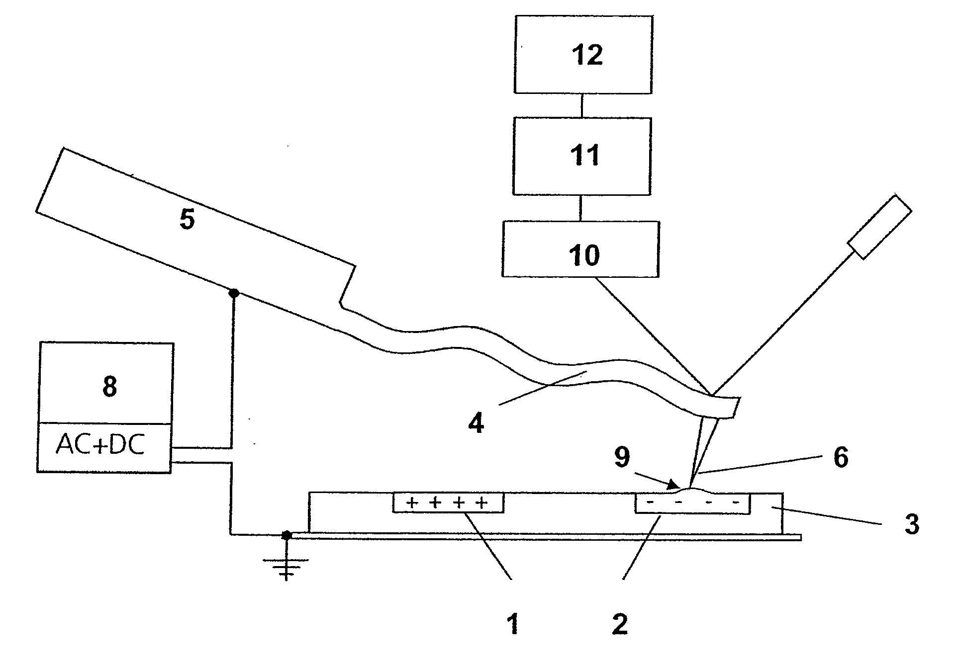
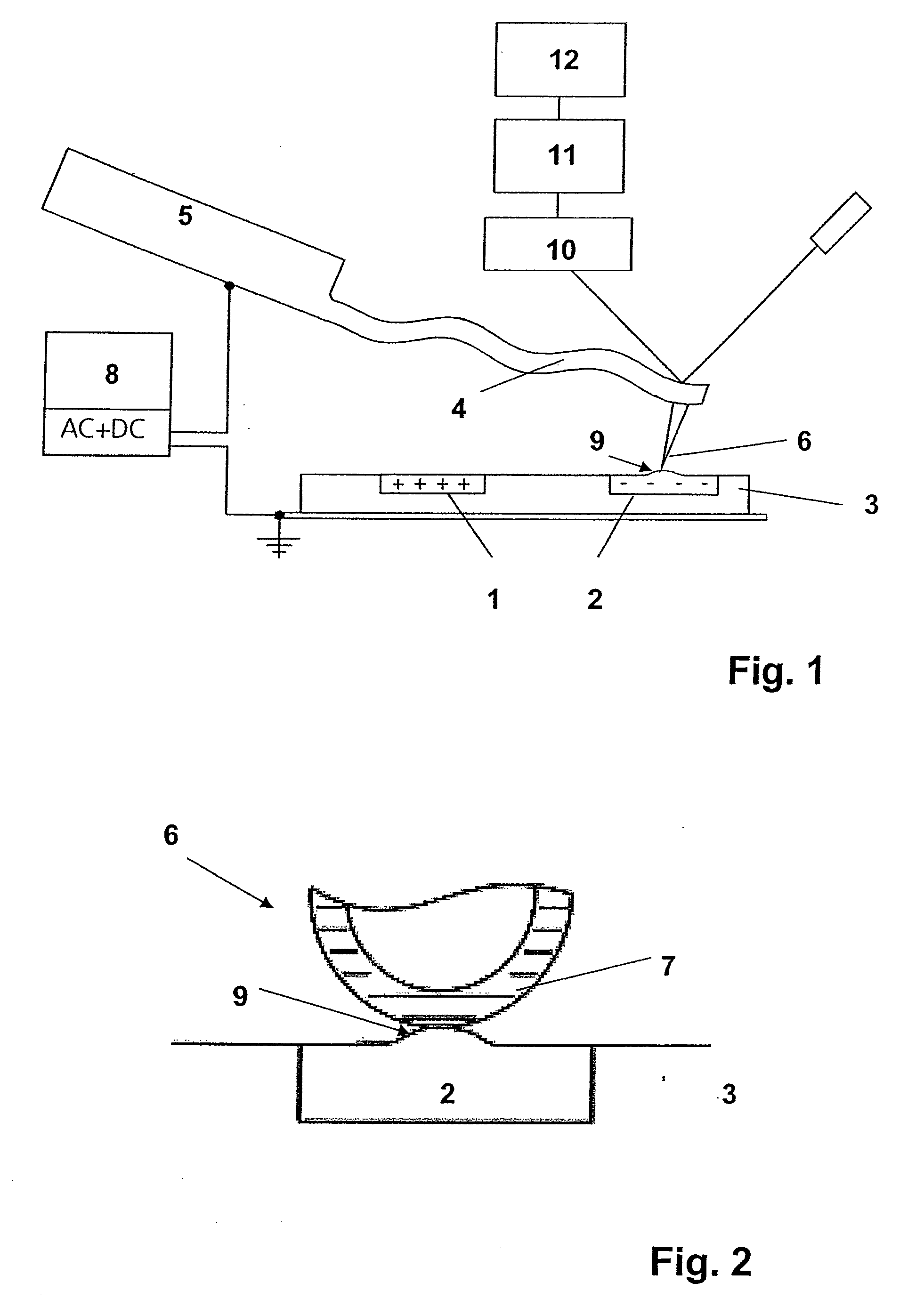
[0023]FIG. 1 shows the experimental setup for detecting doped regions 1 and 2 depending on whether they are positively or negatively doped, of a semiconductor sample 3. The device for investigating or determining the dopant concentration in the respective semiconductor regions 1 and 2 does not differ from a scanning microscope arrangement known per se, in which a leaf spring 4 clamped on one side, usually connected on one side to a chip 5, is scanned over the surface of the semiconductor probe 3. At the free end of the leaf spring 4 there is provided a sensor tip 6 which, in the method according to the invention for determining dopant concentration is brought into contact with the semiconductor sample 3, especially with the doped regions 1 and 2. The sensor tip 6, which mostly consists of silicon and is shown in a detailed cross-sectional view in FIG. 2 is surrounded with a metallic electrically conductive coating 7. Through contact of the sensor tip 6 with, for example, the doped r...


PUM


Abstract

A method is described for determining a dopant concentration on a surface and/or in layer region lying close to the surface of a semiconductor sample using an atomic force microscope, whose leaf-spring tip is brought into contact with the semiconductor sample, forming a Schottky barrier, wherein an electric alternating potential is applied between the spring-leaf tip and the semiconductor sample in the region of the Schottky barrier in such a way that a space charge region inside the semiconductor sample defining the three-dimensional extension of the Schottky barrier is excited and begins to oscillate within the confines of its spatial extension, said oscillations are transmitted to the leaf-spring, are detected and form the basis for determining the dopant concentration.

Description

BACKGROUND OF THE INVENTION[0001]1. Field of the Invention[0002]The invention relates to a method for determining a dopant concentration on a surface and / or in layer region lying close to the surface of a semiconductor sample using an atomic force microscope.[0003]2. Description of the Prior Art[0004]One possibility for doping a semiconductor is the ion implantation method, in which atoms and molecules are ionized, accelerated in an electric field and shot into a solid. The depth of penetration of the ions into the solid depends on their energy, which is typically between several keV and several MeV, and their mass, as well as the mass of the atoms of the solid. Thus, the average range of 10 keV phosphorus ions in silicon is approximately 14 nm and of 1 MeV boron ions in silicon 1.8 μm. By ion bombardment of a solid, it is possible to vary many properties such as electrical and optical properties of a solid, variation in volume, mechanical stresses in the solid surface or the near-s...

Claims


Application Information

Patent Timeline
IPC IPC(8): G01N13/16G01Q60/36G01Q10/00G01Q60/18G01Q60/30G01Q60/32G01Q60/40
CPCB82Y35/00G01Q60/40G01Q60/32G01Q60/30
Inventor ARNOLD, WALTERSCHWARZ, KERSTINRABE, UTE
Owner FRAUNHOFER GESELLSCHAFT ZUR FOERDERUNG DER ANGEWANDTEN FORSCHUNG EV
Why Eureka
Try Eureka