
Connection structure and method of producing the same

a technology of connection structure and connection structure, which is applied in the direction of printed circuit manufacturing, sustainable manufacturing/processing, final product manufacturing, etc., can solve the problems of poor productivity, difficult to adapt to the current technology of forming solder bumps, and poor reliability of screen printing, so as to improve yield and improve production efficiency. , the effect of excellent reliability

Active Publication Date: 2009-04-23
PANASONIC CORP
View PDF27 Cites 24 Cited by
  • Summary
  • Abstract
  • Description
  • Claims
  • Application Information

AI Technical Summary

Benefits of technology

[0083]As described above, with the connection structure and the method of producing the same of the present invention, a connection structure with excellent reliability such as a package can be realized that ensures sure connection between the second plate body (a semiconductor chip, for example) and the first plate body (a wiring board, for example) and the insulation between adjacent terminals that is ready for a narrow-pitch configuration. Since the state of connection between the opposed connection terminals (“connection terminals” implies electrode terminals) of the first and second plate bodies can be made uniform, the effects of increasing the yield and enhancing the production efficiency are generated, too.
[0095]Still further, in the step of sandwiching the conductive substance between the opposed terminals, the distance between the opposed terminals may be controlled, but in the step of sandwiching or embedding the conductive substance between the opposed terminals by pressing the plate bodies, the control of the distance between the opposed terminals is unnecessary, and therefore, the simplification of the process and the device configuration can be achieved.

Problems solved by technology

However, in order to mount a next-generation LSI having over 5000 electrode terminals onto a wiring board, it is necessary that solder bumps corresponding to a narrow pitch of 100 μm or less should be formed on the wiring board, but it is difficult to adapt to it with a current technique for forming solder bumps.
The plating is suitable for a narrow pitch, but has a problem in productivity due to its complicated process.
On the other hand, the screen printing has excellent productivity, but is not suitable for narrowing a pitch because of the use of a mask.
Because of this, there also have been problems of an increase in the number of steps and a decrease in a yield.

Method used


Image

  • Connection structure and method of producing the same
  • Connection structure and method of producing the same
  • Connection structure and method of producing the same

Examples


embodiment 1

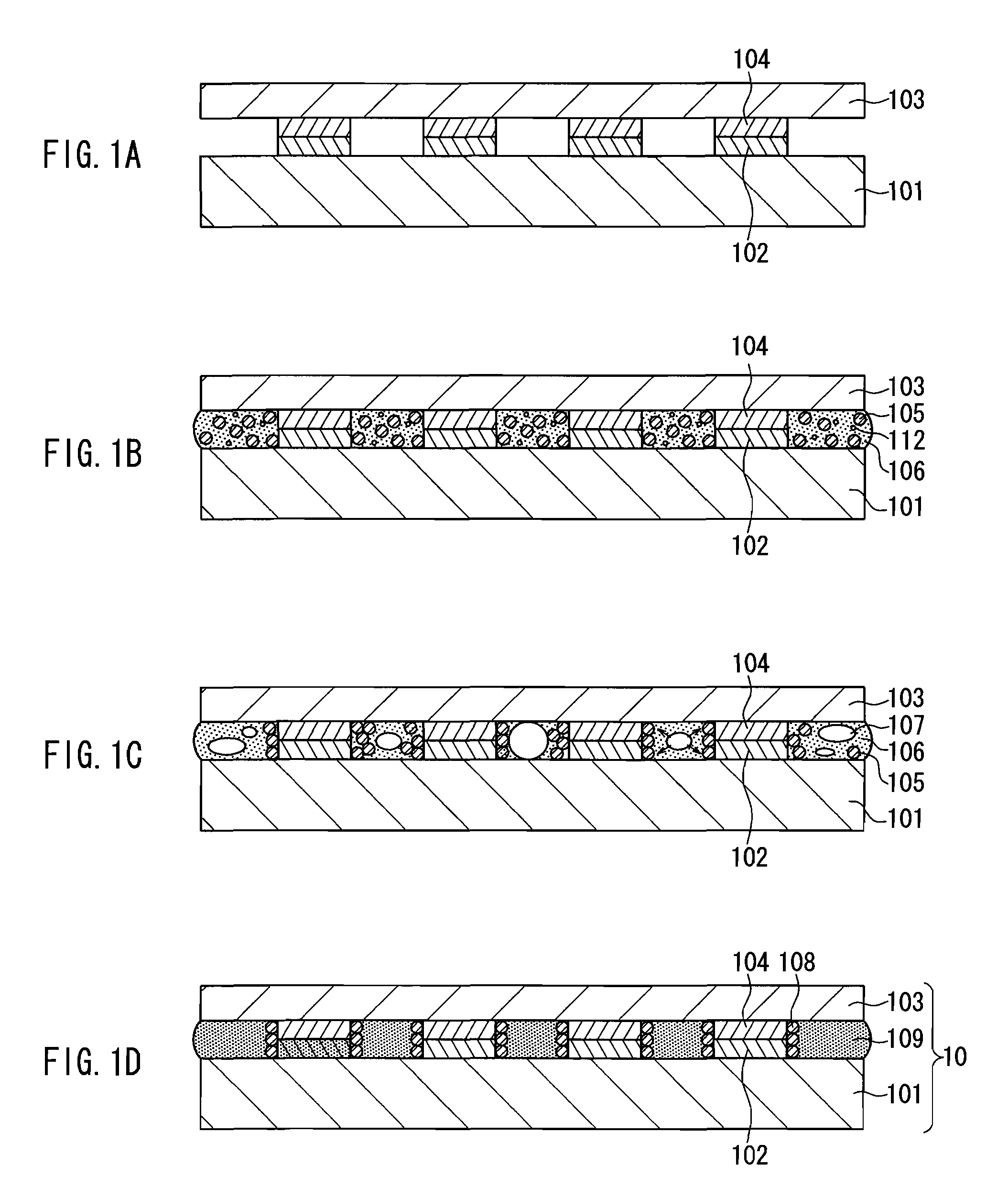
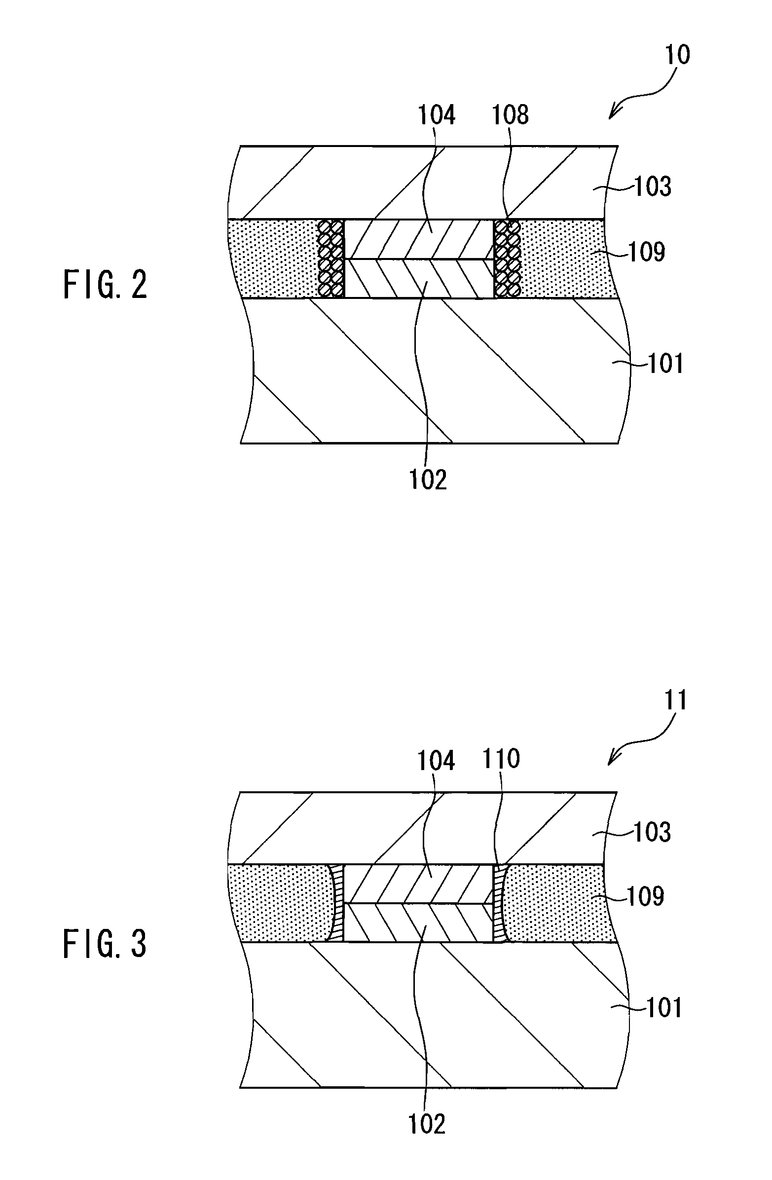
[0123]The following describes a package 10 and a packaging method thereof according to Embodiment 1, while referring to FIGS. 1 and 2.

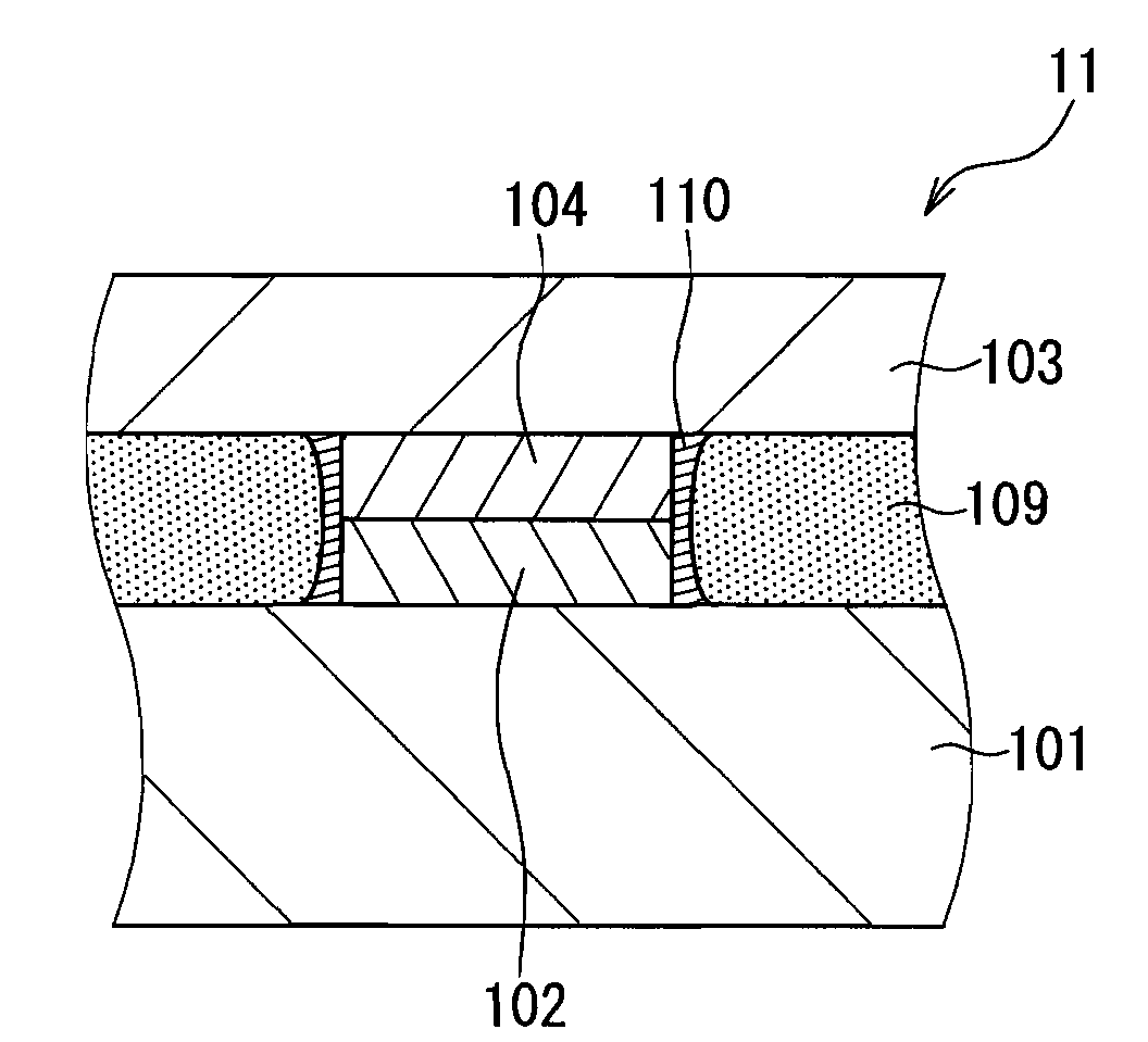
[0124]In FIGS. 1 and 2, “10” denotes a package according to Embodiment 1. “101” denotes a first plate body. “102” denotes a connection terminal formed in a form of a projection on the first plate body. “103” denotes a second plate body. “104” denotes an electrode terminal as one type of the connection terminal in a form of a projection formed on the second plate body. “105” denotes a conductive substance. “106” denotes a resin composition. “107” denotes a bubble. “108” denotes an accumulation of the conductive substance 105 on side faces of the terminals 102 and 104 opposed to each other. “109” denotes a hardened resin composition 106. “112” denotes a convective additive. The package 10 according to Embodiment 1 has a configuration as follows: a plurality of connection terminals 102 formed on the first plate body 101, and a plurality of electrode term...

embodiment 2

[0150]The following describes a package 12 and a packaging method thereof according to Embodiment 2, as an embodiment of the connection structure and the method of producing the same of the present invention, while referring to FIGS. 4, 5, and 6. It should be noted that regarding constituent elements employed in Embodiment 2, if constituent elements like those of Embodiment 1 described above are employed, these constituent elements can achieve effects identical to the effects achieved by the corresponding constituent elements of Embodiment 1 described above, respectively. Therefore, if these constituent elements are identical to those of Embodiment 1, duplicate detail descriptions are omitted in some cases.

[0151]FIGS. 4A to 4E are schematic cross-sectional views of principal steps for producing the package 12 and a state of the same upon completion according to Embodiment 2. In FIGS. 4C to 4E, “111” denotes a conductive substance 105 interposed and embedded between top faces of conn...

example 1

[0182]A connection structure (package 10) according to Embodiment 1 described above with reference to FIGS. 1A to 1D and 2 was produced.

[0183]The first and second plate bodies 101 and 103 in FIG. 1 referred to in conjunction with Embodiment 1 described above were formed as follows: the first plate body 101 was formed with a four-layer-wiring resin multilayer substrate having an Interstitial Via Hole (IVH) structure in all layers, that is, an “ALIVH” substrate (produced by Panasonic Electronic Devices Co., Ltd.); and, a semiconductor chip (a silicon memory semiconductor with a thickness of 0.3 mm and a size of 10 mm×10 mm, having electrode terminals 104 having identical sizes to those of the connection terminals 102 of the first plate body 101, at positions opposed to the connection terminals 102) used as the second plate body 103 was arranged to be opposed to a wiring layer (thickness: 12 μm, diameter: 50 μm, pitch: 100 μm, 352 terminals) that function as the connection terminals 10...


PUM


Abstract

A connection structure (package 10) has a first plate body 101 and a second plate body; in the first plate body 101, a wiring pattern having a plurality of connection terminals 102 is formed, and the second plate body has at least two connection terminals (electrode terminals 104) arranged facing the connection terminals of the first plate body 101. The connection terminals of the first and second plate bodies are connection terminals formed as projections on the surfaces of the first and second plate bodies. A conductive substance 108 is accumulated to cover at least a part of each side face of the connection terminals opposed to each other of the first and second plate bodies, and the connection terminals thus opposed are connected to each other via the conductive substance. The package thus formed is ready for a high-pin-count, narrow-pitch configuration of a next-generation semiconductor chip, and exhibits excellent productivity and reliability. The present invention is advantageous for such a package, for a connection structure applicable to the production of the package, and for a method of producing the connection structure.

Description

TECHNICAL FIELD[0001]The present invention relates to a connection structure in which one plate body having a plurality of connection terminals and another plate body having a plurality of connection terminals (here, the term “connection terminal” also implies electrode terminals) are opposed to each other and the connection terminals of the opposed plate bodies are connected electrically, and also relates to a method of producing the connection structure. The present invention particularly relates to a high-productivity flip-chip package that is ready for a narrow-pitch semiconductor chip, to a connection structure applicable to a flip-chip mounting method, and to a method of producing the connection structure.BACKGROUND ART[0002]In recent years, with a trend toward a higher density and a higher degree of integration of semiconductor integrated circuits (LSI) used in electronic equipment, the number of pins of the electrode terminals of an LSI chip has been increased and the pitch ...

Claims


Application Information

Patent Timeline
IPC IPC(8): H01L23/48H01L21/00H01L23/52H01L23/485H01L23/488
CPCH01L24/11H01L2224/83851H01L24/16H01L24/29H01L24/31H01L24/81H01L24/83H01L2224/13099H01L2224/16225H01L2224/293H01L2224/81101H01L2224/81193H01L2224/81801H01L2224/83192H01L2224/83855H01L2924/01005H01L2924/01009H01L2924/01011H01L2924/01013H01L2924/01027H01L2924/01029H01L2924/01033H01L2924/01047H01L2924/0105H01L2924/01056H01L2924/01078H01L2924/01079H01L2924/01082H01L2924/0781H01L2924/14H05K3/323H05K3/3436H05K3/3484H05K3/361H05K3/363H05K2203/083H05K2203/087H01L2924/01006H01L2924/01019H01L2924/01023H01L2924/014H01L2924/0665H01L2224/29101H01L2924/0132H01L2924/1579H01L2224/8192H01L2224/29111H01L2224/16501H01L2224/29339H01L2224/29347H01L2224/2929H01L24/12H01L2924/00H01L2924/01083H01L2224/29311H01L2924/00014H01L2924/00015H01L2924/351H01L2224/83886H05K3/3485Y02P70/50
Inventor SAWADA, SUSUMUNAKATANI, SEIICHIKARASHIMA, SEIJIKITAE, TAKASHI
Owner PANASONIC CORP
Learn More