Laser device

a laser and laser technology, applied in the field of laser devices, can solve the problems of no cosup>2/sup>laser that can output the 10 kw laser with such short pulse oscillation, and the footprint (occupied space) fp further exceeds 100 m, so as to stabilize the laser output, the effect of reducing the disturbance effect of laser light, and reducing the footprint (occupied area) fp

Active Publication Date: 2009-04-23
GIGAPHOTON
View PDF6 Cites 16 Cited by
  • Summary
  • Abstract
  • Description
  • Claims
  • Application Information

AI Technical Summary

Benefits of technology

[0041]If the optical path LR of the high output CO2 laser is exposed to the atmospheric air, the laser light is absorbed by the atmospheric air. This causes the disturbance effect of the laser light, which may poses instability of the laser output. According to the aspect of the present invention, a purge gas (e.g. N2 gas) is introduced into the cover 33 from the purge gas inlet 34 of the cover 33 of the optical element module 30, and the atmospheric air within the cover 33 is purged with the purge gas, whereby the optical path LR of the high output CO2 laser is prevented from being exposed to the atmospheric air. This makes it possible to minimize the disturbance effect of the laser light, and stabilize the laser output. Additionally, if the group of optical elements 31 is exposed to the atmospheric air during the maintenance, the dust is more likely to be attached to the optical elements 31a, 31b, . . . . If the dust is attached to the optical elements 31a, 31b . . . , the dust absorbs the laser light, and hence the optical elements 31a, 31b, . . . may be heated to be damaged. According to the aspect of the present invention, the maintenance of the group of optical elements 31 is performed through the maintenance hatches 35, 36, 37 locally provided to the cover 32. This enables minimizing the possibility that the dust is attached to the group of optical elements 31 due to the exposure to the atmospheric air.
[0042]According to the eleventh aspect of the present invention, as shown in FIG. 6, the housing of the oscillator unit 11 and the housing of the at least one amplifier unit 21, 22, which are made adjoin to each other and whose wide surfaces are made face to each other, are vertically layered. Additionally, the housings of the at least two amplifier units 23, 24, which are made adjoin to each other and whose wide surfaces are made face to each other, are vertically layered. Thus, as shown in FIG. 3, although the area covered by the oscillator unit 11 and the amplifier units 21, 22, 23, 24 is expanded in the vertical direction, the expansion in the horizontal direction can be reduced as compared with the conventional art (FIG. 1), whereby the footprint (occupied area) FP can be greatly reduced as compared with the conventional art (FIG. 1).

Problems solved by technology

However, in the LPP-type EUV light source system that employs CO2 laser as the driver laser device and uses a target formed of tin Sn, only about 1-2% of output can be obtained as the EUV light output from the laser light emitted by the driver laser device.
However, this industrial CO2 laser is not the pulse oscillating laser device necessary for the driver laser device for the EUV light source, but is a CW oscillating laser device.
However, there is no commercially available CO2 laser that can output the 10 kW laser with such short pulse oscillation.
Thus, those oscillator unit and four amplifier units occupy a large floor space in the semiconductor manufacturing lines.
Thus, the footprint (occupied space) FP further exceeds 100 m2, and becomes extremely large.
However, it is practically difficult to reserve a vast area in the floor space in the semiconductor manufacturing line only for the EUV light source, or only for the driver laser device.
This causes a problem that operator bears a large burden because the operator has to walk around each of the separated places to perform adjustment of the alignment of the optical elements, or other maintenance operations, which deteriorates the operating efficiency.
Furthermore, due to the increased optical path and decentralized arrangement of the group of optical elements, the alignment of the optical system is largely affected by the stability of the floor surface and vibration of the floor or slight shock during the maintenance.
For example, in a case where the optical path reaches 40-50 m, the slight displacement of only 100 μm in the transmission optical system results in the displacement of several mm at around the portion where the laser light is outputted, which hinders the efficient amplification and deteriorates the laser output.
This poses a problem that it becomes difficult to guarantee the long-term stability of the laser output in a circumstance where this guarantee is required, such as the semiconductor manufacturing line.
This causes the disturbance effect of the laser light, which may poses instability of the laser output.
. . may be heated to be damaged.

Method used


Image

  • Laser device
  • Laser device
  • Laser device

Examples


first example

[0057]FIG. 3 is a configuration diagram of the laser device 1 of the first example, and shows a top view, as is the case with FIG. 1 that illustrates a conventional art. FIGS. 4A and 4B are diagrams showing examples of inner configurations of the oscillator unit 11 and the amplifier units 21, 22, 23, 24 of the first example, respectively. FIGS. 51A and 51B are diagrams showing other examples of inner configurations of the amplifier units 21, 22, 23, 24 of the first example, respectively. FIG. 6 is a perspective view illustrating the laser device 1 of the first example as viewed from the front surface side. FIG. 7 is a perspective view illustrating an external appearance of the optical element module 30 of the laser device 1 of the first example.

[0058]As shown in FIGS. 3 and 6, the laser device 1 of the first example comprises one oscillator unit 11, four amplifier units 21, 22, 23, 24, a group of optical elements 31, power supplies 41, 42, 43, 44, 45 respectively for the oscillator ...

second example

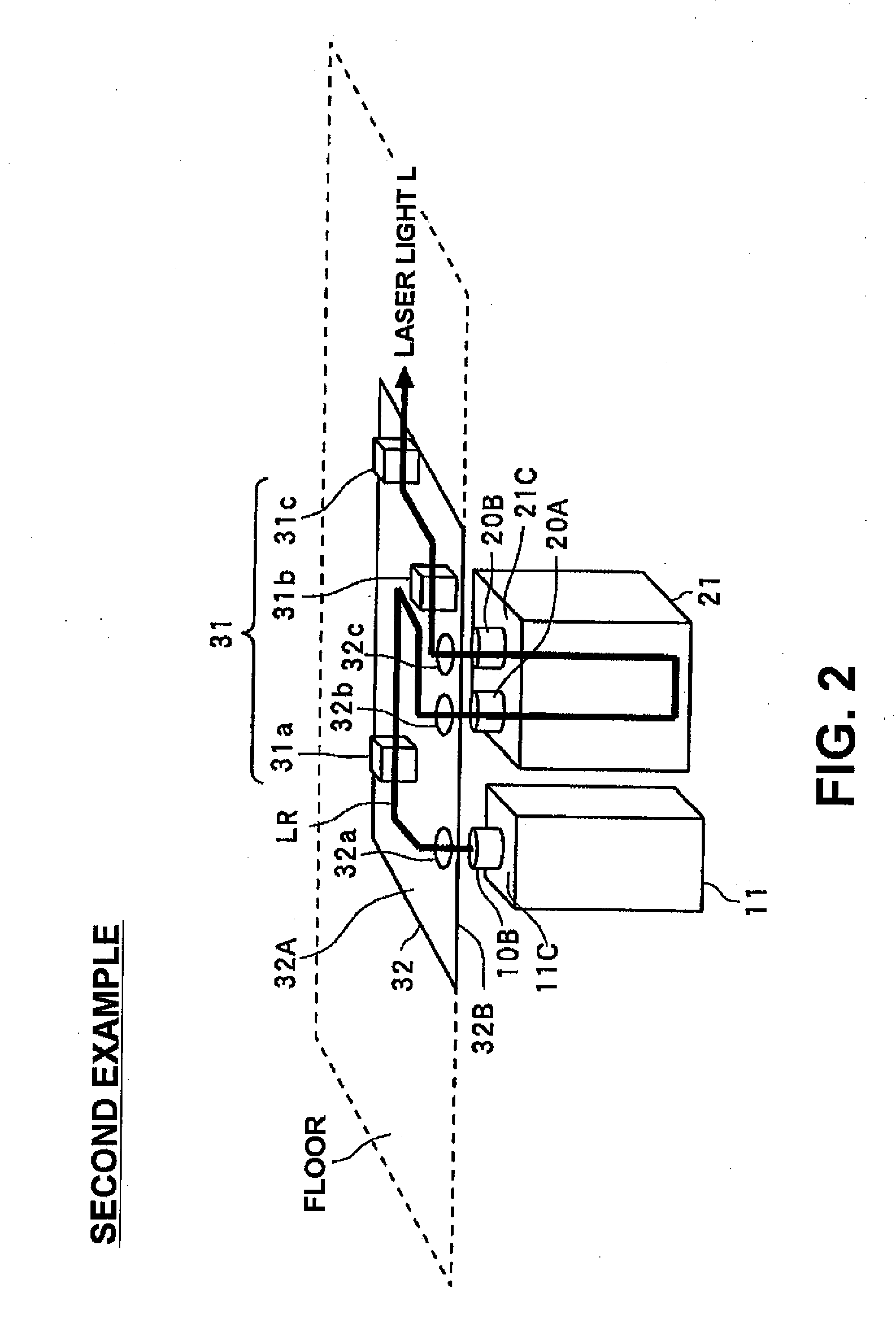
[0093]FIG. 2 is a perspective view showing a configuration of a second example. The housings of the oscillator unit 11 and the amplifier unit 21 are placed below the plate 32 of the optical element module 30. The oscillator unit 11, the amplifier unit 21, and the plate 32 are arranged such that the outgoing light from the output port 10B provided to the oscillator unit 11, and the incoming and the outgoing lights passing through the input port 20A and the output port 20B provided to the amplifier unit 21 intersect with the plate 32 via the holes 32a, 32b, 32c formed in the plate 32.

[0094]Thus, the area covered by the oscillator unit 11 and the amplifier 21 is confined within the floor area covered by the plate 32, whereby the footprint (occupied area) FP can be greatly reduced as compared with the conventional art (FIG. 1).

[0095]In FIG. 2, only the housings of the oscillator unit 11 and the amplifier unit 21 are placed below the plate 32 of the optical element module 30. However, it...

third example

[0097]In the first example, the housings of the oscillator unit 11 and the amplifier units 21, 22 are layered in the vertical direction, while the housings of the amplifier units 23, 24 are layered in the vertical direction. Thus, at the time of maintenance of the oscillator unit 11 and the amplifier units 21, 22, 23, 24, the operator may not access the check / maintenance target because of being blocked by the other layered units.

[0098]Thus, it may be possible to provide a maintenance mechanism 90 as shown in FIGS. 8A through 8C to make it possible for the oscillator unit 11 and the amplifier units 21, 22, 23, 24 to be freely drawn toward the rear direction of the optical element module 30, and to enable the operator to access the check or maintenance target.

[0099]FIG. 8A is a diagram illustrating the maintenance mechanism 90 as viewed from a side of the optical element module 30. FIG. 8B is a diagram illustrating the maintenance mechanism 90 as viewed from a rear side of the optical...


PUM


Abstract

A laser device, which includes an oscillator unit having a rectangular-solid-shaped housing containing a laser oscillator for generating and outputting a laser light; an amplifier unit having a rectangular-solid-shaped housing containing an amplifier that receives and amplifies the laser light to output; and, a group of optical elements including optical elements provided on a laser light path, wherein the laser device includes one or more amplifier units, and the oscillator and the amplifier units are arranged such that surfaces having a wide area other than a surface having a smallest area of a housing of the oscillator unit and a housing of at least one amplifier unit are next to and face each other, or such that surfaces having a wide area other than a surface having a smallest area of a housing of at least two amplifier units are next to and face each other.

Description

BACKGROUND[0001]1. Technical Field[0002]The present invention relates to a laser device, more specifically to a laser device used for a driver of an EUV light source.[0003]2. Related Art[0004]To achieve higher density LSI, the photolithography technology, in which a circuit pattern is optically transferred on a semiconductor wafer, plays an important role. In the photolithography process, a reduced-projection-exposure device, called a stepper, is mainly employed. In other words, with the reduced projection light system, a transmitted light having an original pattern (reticle) emitted by a light source is projected to a light-sensitive material on a semiconductor substrate, and the circuit pattern is formed. The resolution of this projected image depends on the wavelengths of the light source used. Thus, with the increasing demand for finer pattern line width, the wavelength of the light source is shortened to an ultraviolet range.[0005]Recently, as light sources, KrF excimer laser (...

Claims


Application Information

Patent Timeline
Patent Type & Authority Applications(United States)
IPC IPC(8): H01S3/30
CPCG03F7/70033G03F7/70975H01S3/03H01S3/2308H01S3/041H01S3/2232H01S3/0346
Inventor ABE, TAMOTSUHOSHINO, HIDEO
Owner GIGAPHOTON
Why Eureka
Try Eureka