Method of Manufacturing Light-Emitting Device, and Evaporation Donor Substrate

a technology of light-emitting devices and donor substrates, which is applied in the manufacture of electric discharge tubes/lamps, electric system manufacture, transportation and packaging, etc., can solve the problems of increasing the region of the transfer layer, which is to be transferred, and achieves improved definition, high precision, and increased pixels

Active Publication Date: 2009-04-23
SEMICON ENERGY LAB CO LTD
View PDF23 Cites 64 Cited by
  • Summary
  • Abstract
  • Description
  • Claims
  • Application Information

AI Technical Summary

Benefits of technology

[0022]Application of the present invention makes it easy to form a layer containing an evaporation material for forming a light-emitting element and to manufacture a light-emitting device including the light-emitting element.
[0023]In addition, application of the present invention makes it possible to form a f

Problems solved by technology

There is a problem in that a region in the transfer layer, which is to be transferred, in

Method used


Image

  • Method of Manufacturing Light-Emitting Device, and Evaporation Donor Substrate
  • Method of Manufacturing Light-Emitting Device, and Evaporation Donor Substrate
  • Method of Manufacturing Light-Emitting Device, and Evaporation Donor Substrate

Examples


embodiment mode 1

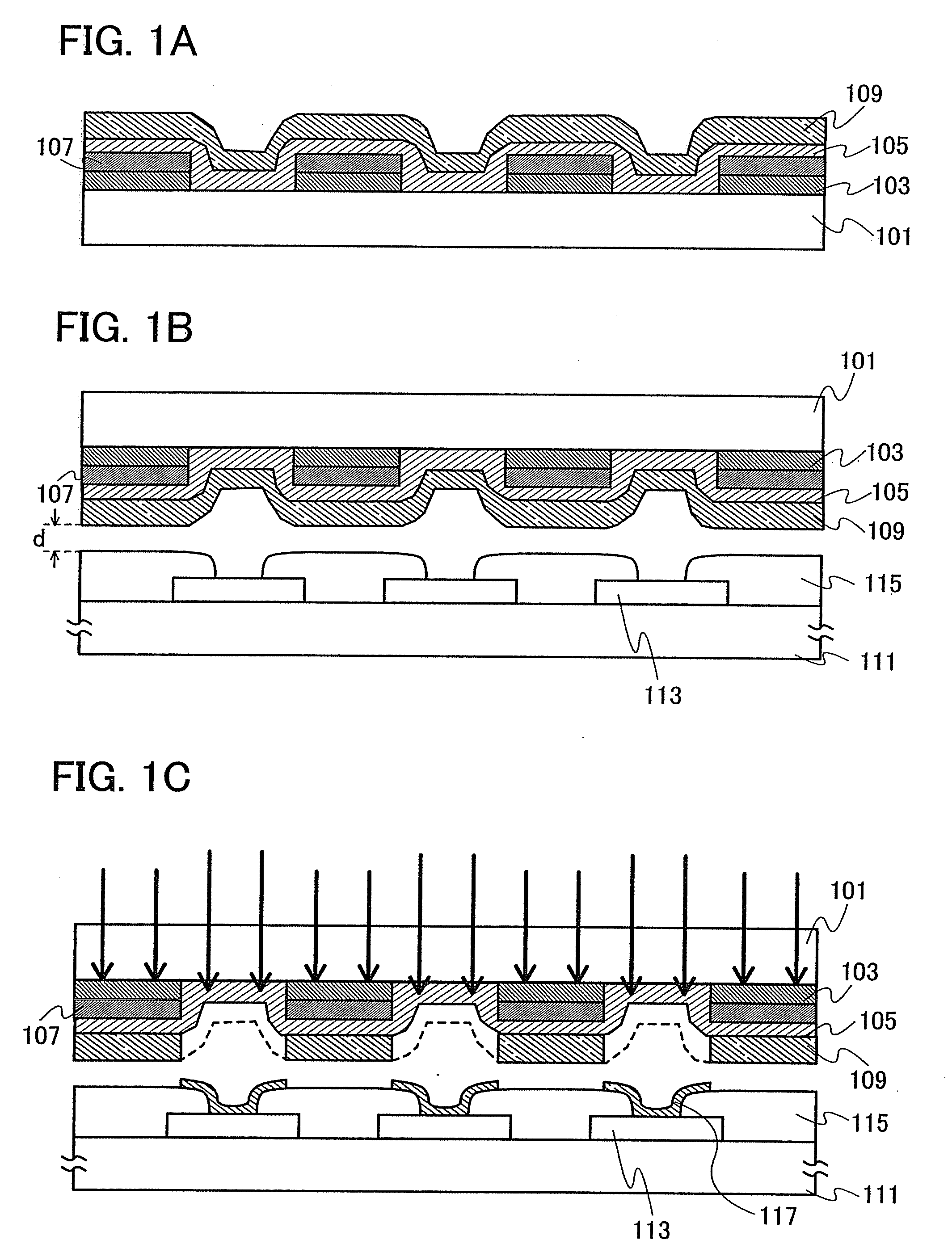
[0045]An evaporation donor substrate and a manufacturing method of a light-emitting device of the present invention are described using FIGS. 1A to 1C.

[0046]FIG. 1A shows one example of an evaporation donor substrate of the present invention. In FIG. 1A, a reflective layer 103 is formed over a first substrate 101 which is a supporting substrate. The reflective layer 103 includes an opening portion. In addition, a heat insulating layer 107 is formed over the reflective layer 103 and includes an opening portion in a region overlapped with the opening portion included in the reflective layer 103. In addition, a light absorption layer 105 is formed over the heat insulating layer 107. In FIGS. 1A to 1C, the light absorption layer 105 is formed so as to cover the entire surface of the first substrate 101. In addition, over the light absorption layer 105, a material layer 109 containing an evaporation material is formed.

[0047]Note that in this specification, “overlapped with” means not onl...

embodiment mode 2

[0092]In this embodiment mode, an evaporation donor substrate of the present invention, which differs in structure from the evaporation donor substrate in the above embodiment mode, is described. Note that when there is no particular description, the evaporation donor substrate described in this embodiment mode is formed using a material and a manufacturing method similar to the material and the method in the above embodiment mode.

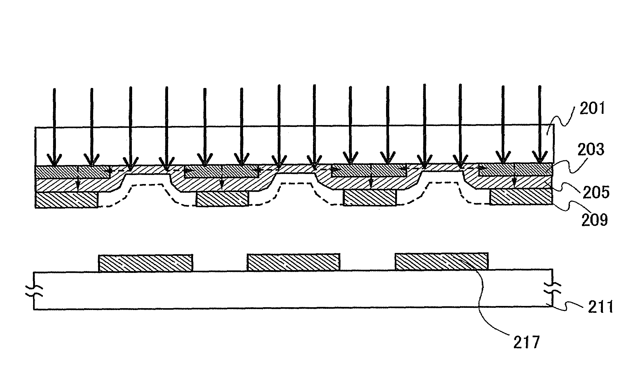
[0093]FIG. 3A shows one example of an evaporation donor substrate of the present invention. In FIG. 3A, the reflective layer 103 including an opening portion is formed over the first substrate 101 which is the supporting substrate. In addition, the light absorption layer 105 is formed over the entire surface of the first substrate 101 so as to cover the opening portion in the reflective layer 103. The heat insulating layer 107 is formed over the light absorption layer 105 and includes an opening portion in a region overlapped with the opening portion inclu...

embodiment mode 3

[0106]In this embodiment mode, a manufacturing method of a full-color display device by using any evaporation donor substrate used in the above embodiment modes is described.

[0107]Although an example in which deposition is performed onto adjacent the first electrode layers 113 in a single deposition process is described in each of Embodiment Modes 1 and 2, when a full-color display device is manufactured, light-emitting layers for emitting light of different colors are formed in different regions through a plurality of deposition steps.

[0108]A manufacturing example of a light-emitting device capable of full color display is described below. Here, an example of a light-emitting device using light-emitting layers for emitting light of three colors is described.

[0109]Three evaporation donor substrates shown in FIG. 1A, FIG. 2B, FIG. 3A, or FIG. 3C are prepared. In the evaporation donor substrates, layers containing different kinds of evaporation materials are formed. Specifically, a fi...


PUM

PropertyMeasurementUnit
Thicknessaaaaaaaaaa
Thicknessaaaaaaaaaa
Thicknessaaaaaaaaaa

Abstract

The present invention provides a method of manufacturing a light-emitting device and an evaporation donor substrate, by which the precision of patterning of an EL layer of each color can be improved in manufacture of a full color flat panel display using emission colors of red, green, and blue. A first substrate which includes a reflective layer including an opening portion, a heat insulating layer including an opening portion in a position overlapped with the opening portion of the reflective layer over the reflective layer, a light absorption layer covering the opening portion of the reflective layer and the opening portion of the heat insulating layer over the heat insulating layer, and a material layer over the light absorption layer is used. While one surface of the first substrate is disposed close to a deposition target surface of a second substrate, the first substrate is irradiated with light from the other surface of the first substrate. The irradiation light is absorbed in the light absorption layer in the position overlapped with the opening portion of the reflective layer to heat an evaporation material. The heated evaporation material is evaporated onto the second substrate.

Description

BACKGROUND OF THE INVENTION[0001]1. Field of the Invention[0002]The present invention relates to a light-emitting device and a method of manufacturing the light-emitting device. The present invention also relates to an evaporation donor substrate used for deposition of a material which can be deposited onto a substrate.[0003]2. Description of the Related Art[0004]Organic compounds can take various structures compared with inorganic compounds, and it is possible to synthesize materials having various functions by appropriate molecular design. Owing to these advantages, photo electronics and electronics which utilize functional organic materials have been attracting attention in recent years.[0005]A solar cell, a light-emitting element, an organic transistor, and the like are given as examples of electronics devices using an organic compound as a functional organic material. These devices take advantage of electrical properties and optical properties of the organic compound. Among the...

Claims


Application Information

Patent Timeline
IPC IPC(8): H01J9/00B32B9/00
CPCH01L51/0013H01L51/0037H01L51/0052H01L51/0059Y10T428/24331H01L51/0078H01L51/5012H01L51/5048H01L51/5088H01L51/007C23C14/048Y10T428/31504H10K71/18H10K85/1135H10K85/6565H10K85/615H10K85/631H10K85/311H10K50/14H10K50/17H10K50/11H05B33/10B41M5/38242B41M5/382
Inventor AOYAMA, TOMOYASATO, YOSUKEYOKOYAMA, KOHEITAKAHASHI, RENA
Owner SEMICON ENERGY LAB CO LTD
Why Eureka
Try Eureka