

Method for manufacturing bonded wafer
a technology of bonded wafers and manufacturing methods, applied in the direction of semiconductor/solid-state device manufacturing, basic electric elements, electric apparatus, etc., can solve the problems of deteriorating electric characteristics of semiconductor devices, and achieve the effect of reducing costs
Active Publication Date: 2009-04-30
SHIN-ETSU HANDOTAI CO LTD
View PDF9 Cites 19 Cited by
- Summary
- Abstract
- Description
- Claims
- Application Information
AI Technical Summary
Benefits of technology
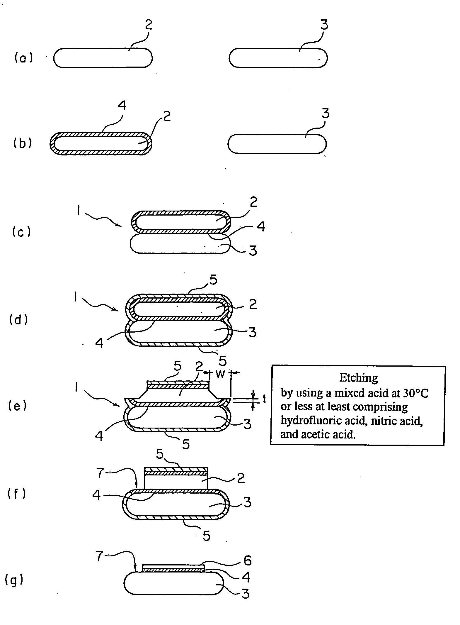
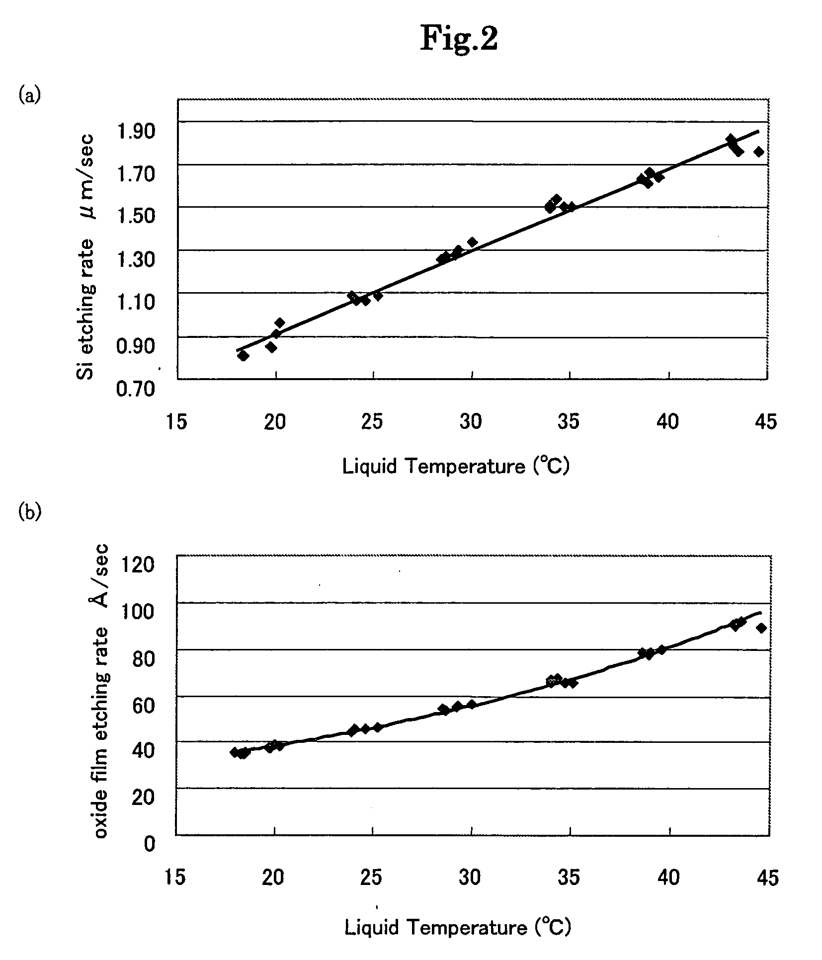
The present invention provides a method for manufacturing a bonded wafer that removes the unbonded portion of the outer periphery of the bond wafer without causing metallic contamination and maintaining the electric characteristics of semiconductor devices. The method involves forming an oxide film on at least one surface of the base wafer or the bond wafer, bringing them into close contact via the oxide film, subjecting them to a heat treatment under an oxidizing atmosphere to bond them together, grinding and removing the outer periphery of the bond wafer so that it has a predetermined thickness, subsequently removing an unbonded portion of the outer periphery of the bond wafer by etching, and then thinning the bond wafer to a desired thickness. The etching is conducted using a mixed acid at -30°C or less, which has a high selectivity ratio between the etching rate against Si and SiO2, and does not damage the base wafer. This method allows for the efficient removal of the unbonded portion of the outer periphery of the bond wafer while maintaining its quality.
Problems solved by technology
It has turned out, however, that removing the unbonded portion by alkaline etching causes metallic contamination, and which can deteriorate electric characteristics of semiconductor devices.
Method used
View moreImage
Smart ImageViewing Examples

Examples
examples
[0047]Hereinafter, Examples of the present invention will be described. However, the present invention is not restricted thereto.
Login to View More PUM
 Abstract
The present invention provides a method for manufacturing a bonded wafer comprising steps of forming an oxide film on at least a surface of a base wafer or a surface of a bond wafer; bringing the base wafer and the bond wafer into close contact via the oxide film; subjecting these wafers to a heat treatment under an oxidizing atmosphere to bond the wafers together; grinding and removing the outer periphery of the bond wafer so that the outer periphery has a predetermined thickness; subsequently removing an unbonded portion of the outer periphery of the bond wafer by etching; and then thinning the bond wafer so that the bond wafer has a desired thickness, wherein the etching is conducted by using a mixed acid at 30° C. or less at least comprising hydrofluoric acid, nitric acid, and acetic acid. Thus there is provided a method for manufacturing a bonded wafer by which unbonded portions of the outer periphery of the bond wafer are removed with a high selectivity ratio (RSi / RSiO2) without causing metallic contamination.
Description
TECHNICAL FIELD[0001]The present invention relates to a method for manufacturing a bonded wafer, in particular to a method of etching the unbonded portion of the outer periphery of the bond wafer.BACKGROUND ART[0002]Bonded wafers are used as wafers for high performance devices. Each of the bonded wafers is manufactured by bonding a semiconductor wafer with another wafer or the like and then thinning the wafer on the side where devices are fabricated.[0003]Specifically, for example, two mirror-polished silicon wafers are prepared, and an oxide film is formed at least on one of the wafers. Then these wafers are brought into close contact to each other and subjected to a heat treatment at a temperature of from 200 to 1200° C. to increase bonding strength. After that, the wafer on the side where devices are fabricated (a bond wafer) is ground, polished and the like to thin the wafer so that the bond wafer has a desired thickness. As a result, a bonded SOI wafer comprising an SOI (Silico...
Claims
Login to View More Application Information
Patent Timeline
 Patent Type & AuthorityApplications(United States)
IPC IPC(8): H01L21/302H01L21/02
CPCH01L21/76256
InventorOKABE, KEIICHIMIYAZAKI, SUSUMU
OwnerSHIN-ETSU HANDOTAI CO LTD