Conversion device, conversion method, program, and recording medium

a conversion device and conversion method technology, applied in error detection/correction, instruments, detecting faulty computer hardware, etc., can solve problems such as controllability over pseudo primary input lines and observation of pseudo primary output lines, and achieve the effects of reducing power consumption during test, reducing the size of test patterns, and reducing the size of transition delay faults

Inactive Publication Date: 2009-04-30
JAPAN SCI & TECH CORP +2
View PDF7 Cites 7 Cited by
  • Summary
  • Abstract
  • Description
  • Claims
  • Application Information

AI Technical Summary

Benefits of technology

[0038]According to the present invention, since an efficient technique of reducing the size of test patterns by compaction for detecting transition delay faults is realized, it is possible to reduce of transition delay fault by remedying the problem of the increase of the size of test patterns for detecting transition delay faults.
[0039]Besides, according to the present invention, it is also possible to reduce the power consumption during test by converting a test pattern into a test pattern which reduces power consumption during test. This is useful to prevent the yield from decreasing.
[0040]Further, according to the present invention, it is also possible to add new characteristics such as being compacted to a converted test pattern without losing the fault coverage of an initial test pattern given in ahead.
[0041]Further, according to the present invention, since the size of test patterns for detecting delay faults gets smaller, it is also possible to execute tests to detect delay faults which have been impossible to execute tests enough because the test pattern sizes are so large that their test takes too much time. Therefore, the quality of semiconductor devices improves by executing tests of defective semiconductor devices which have been shipped as non-defective products because of shortage of tests.
[0042]Further, the method of the present invention is applicable to overall semiconductor devices to which full scan design is applied because the method does not depend on the system of scan circuit, the kind of clocks, or the number of clocks. That is, the method is also applicable to semiconductor devices which have a plurality of scan chains, to semiconductor devices which have a plurality of clocks which drive scan circuits, and to semiconductor devices whose timing are various to load values from the combinational circuit portion of the full-scan sequential circuit to flip flops.

Problems solved by technology

Due to this, to test the combinational circuit portion 1201 has problems of controllability over the pseudo primary input lines and observability of the pseudo primary output lines.

Method used


Image

  • Conversion device, conversion method, program, and recording medium
  • Conversion device, conversion method, program, and recording medium
  • Conversion device, conversion method, program, and recording medium

Examples


Embodiment Construction

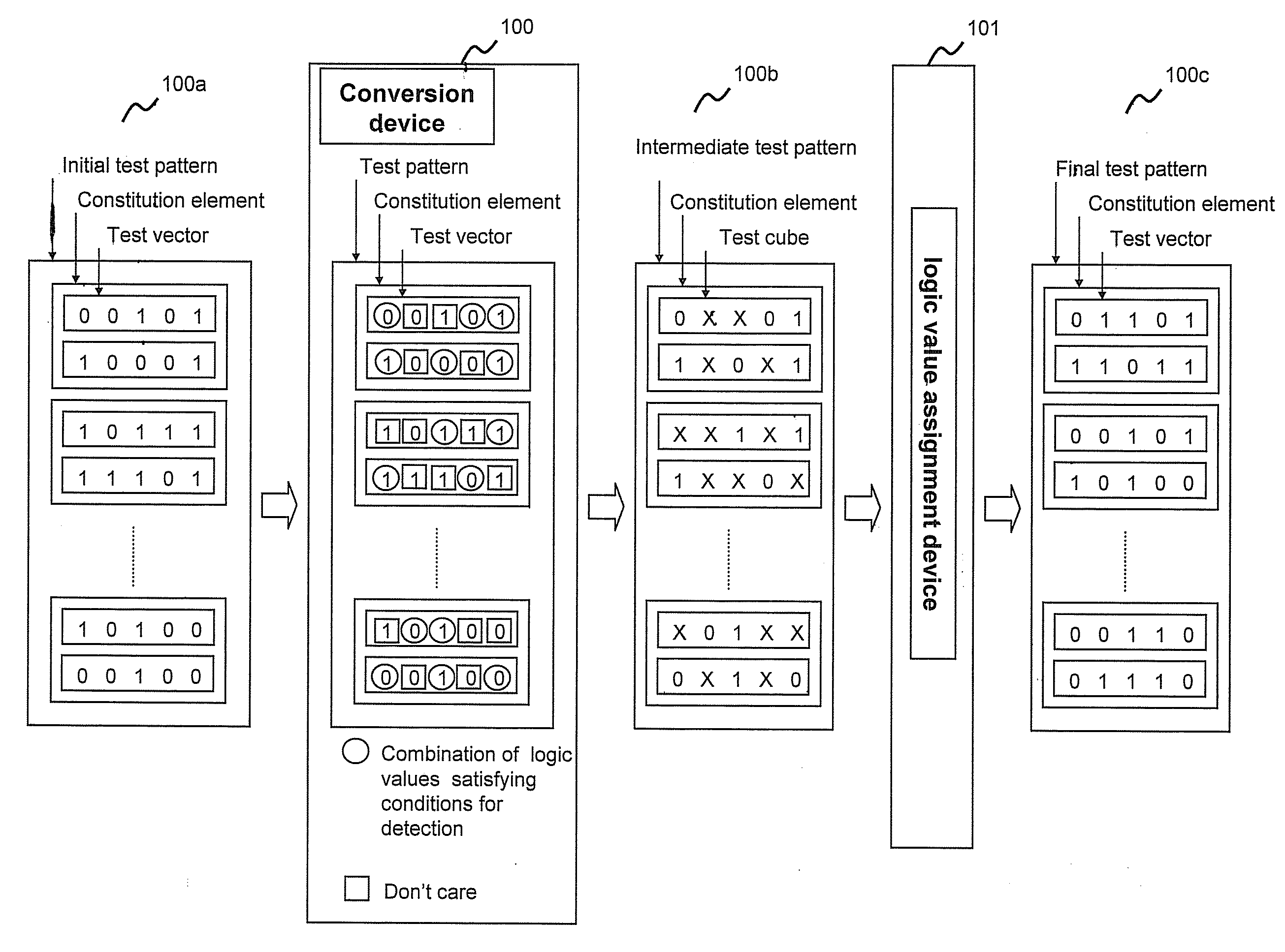
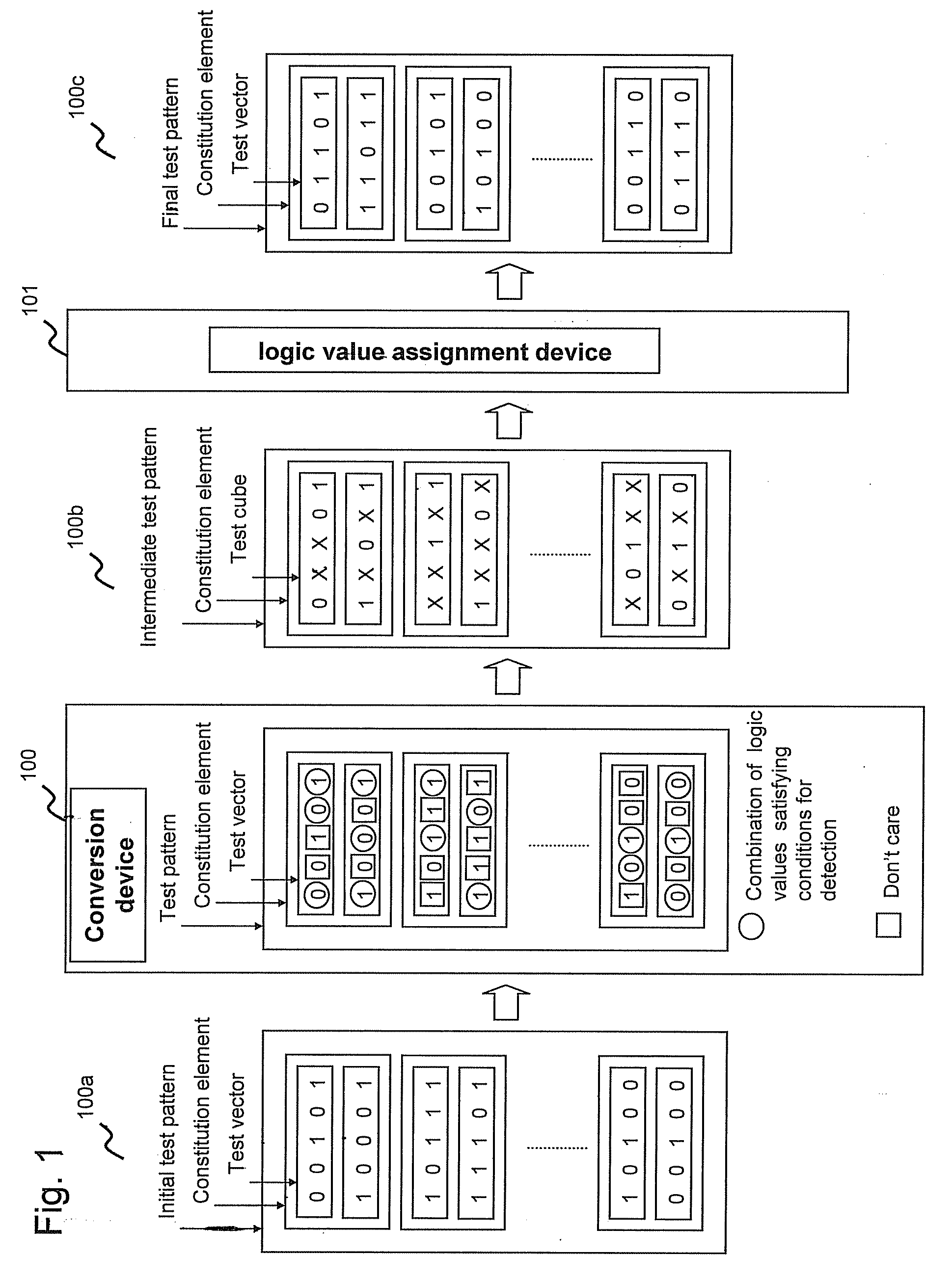
[0057]The summary of the present invention is described below. The present invention is a test technique to assure the performance of at-speed test in the tests of VLSI. And the present invention is essentially means for identifying don't care bits in a test pattern based on information of transition delay faults which can be detected by each test vector of an initial test pattern given in ahead. The present invention is applicable, for example, to compaction of given test patterns by merging each test vector without losing fault coverage. And the present invention can be used not only to compaction of test patterns but also used for other various purposes such as to convert a given test pattern into a test pattern to avoid error of test resulted from power supply voltage drop owing to increase of power consumption during capture mode of scan flip flops.

[0058]FIG. 1 is a schematic diagram of the present invention.

[0059]In FIG. 1, an initial test pattern 100a is a test data given in ...


PUM


Abstract

Provided are a conversion device and the like for converting a initial test pattern given in advance into a test pattern of a bit constitution of different logic values, without losing the fault coverage of transition delay fault which can be detected by the constitution element of the initial test pattern. The conversion device converts an initial test pattern 100a given in advance for a logic circuit into an intermediate test pattern 100b of a bit constitution of different logic values, where the constitution elements of the initial test pattern 100a are at least two test vectors applied in succession. The conversion device includes a decision means for deciding a combination of logic values in the initial test pattern 100a which meet a detection condition of faults of the logic circuit which can be detected by applying the constitution elements.

Description

TECHNICAL FIELD[0001]The present invention relates to a conversion device, a conversion method, a program capable of causing a computer to execute a conversion method, and a recording medium recording this program. More specifically, the present invention relates to a conversion device and the like for converting a test pattern given in ahead for a logic circuit into a test pattern with a different bit constitution of logic values.BACKGROUND ART[0002]Here, an extraction technique of don't care bits in a test pattern suggested conventionally for detecting a stuck-at fault is described.[0003]FIG. 10 is a schematic diagram of a full-scan sequential circuit in an ordinary logic circuit.[0004]Generally, a semiconductor logic circuit is a sequential circuit in most cases. The sequential circuit is configured to include a combinational circuit portion 1201 constituted by logic elements such as an AND gate, a NAND gate, an OR gate and a NOR gate, and flip-flops 1203 each storing a circuit i...

Claims


Application Information

Patent Timeline
Patent Type & Authority Applications(United States)
IPC IPC(8): G01R31/3177G06F11/25
CPCG01R31/318335G01R31/318328
Inventor KAJIHARA, SEIJIMIYASE, KOHEIWEN, XIAQINGMINAMOTO, YOSHIHIRODATE, HIROSHI
Owner JAPAN SCI & TECH CORP
Why Eureka
Try Eureka