Monitoring ionizing radiation in silicon-on insulator integrated circuits

a technology of integrated circuits and ionizing radiation, which is applied in the field of integrated circuit ionizing radiation monitoring, can solve problems such as failure of integrated circuits containing devices, device built in silicon-on-insulator (soi) substrates are particularly sensitive, and the function of various integrated circuit devices may be disrupted

Inactive Publication Date: 2009-04-30
GLOBALFOUNDRIES INC
View PDF7 Cites 7 Cited by
  • Summary
  • Abstract
  • Description
  • Claims
  • Application Information

AI Technical Summary

Problems solved by technology

The functioning of various integrated circuit devices, such as n-channel field effect transistors (NFETs) and p-channel field effect transistors (PFETs) may be disrupted when the device is struck by ionizing radiation.
Disruption of individual devices can lead to failure of the integrated circuit containing the devices.
Devices built in silicon-on-insulator (SOI) substrates are particularly sensitive because charge generated by ionizing radiation is difficult to dissipate.

Method used


Image

  • Monitoring ionizing radiation in silicon-on insulator integrated circuits
  • Monitoring ionizing radiation in silicon-on insulator integrated circuits
  • Monitoring ionizing radiation in silicon-on insulator integrated circuits

Examples


Embodiment Construction

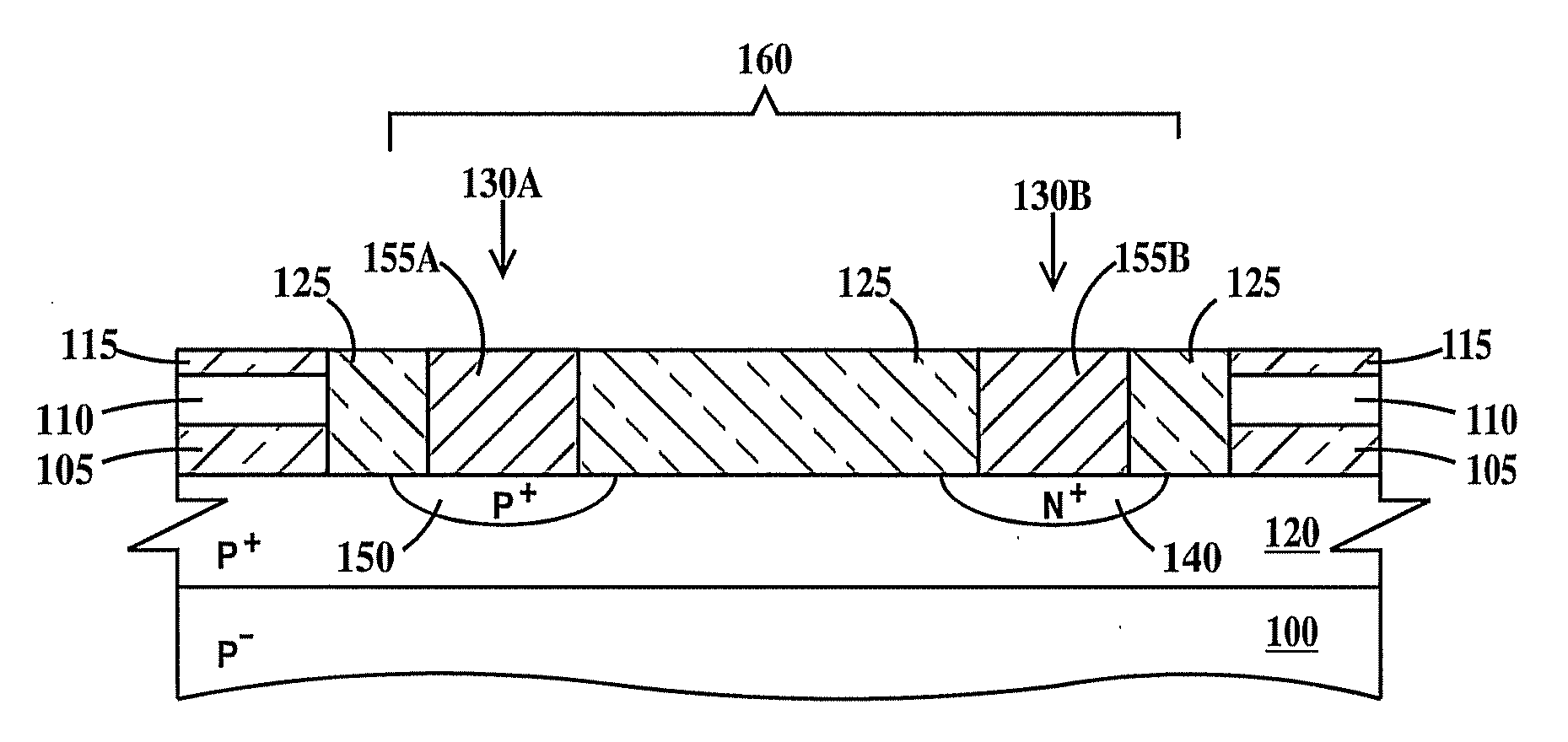
[0016]A domino logic circuit is defined as a clocked (or dynamic) logic circuit including a latch that has a pre-chargeable node. An ionizing radiation is defined as radiation that will generate hole-electron pairs in N or P type doped silicon. Examples of ionizing radiation include but are not limited to protons, alpha particles, gamma rays, X-rays and cosmic rays.

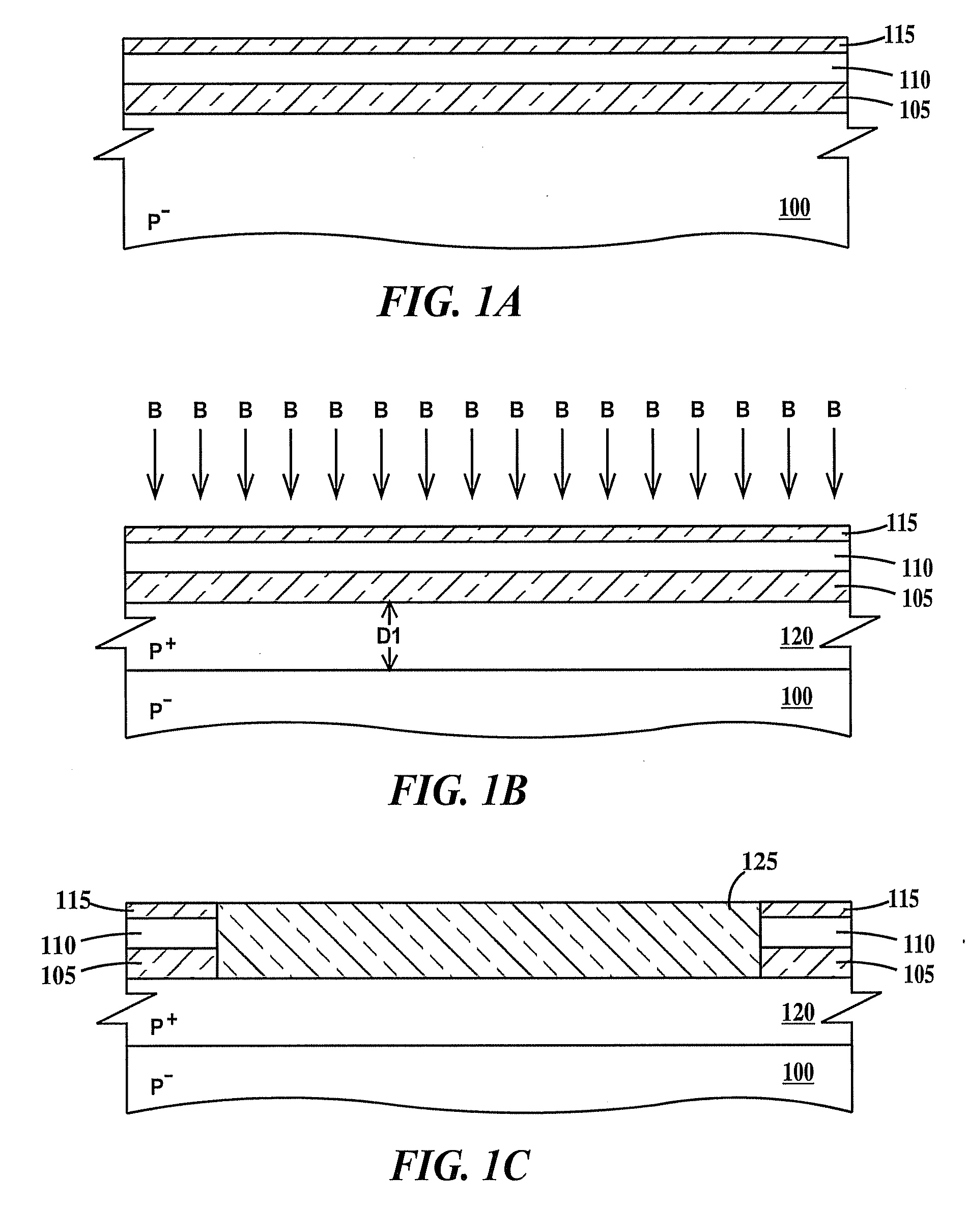
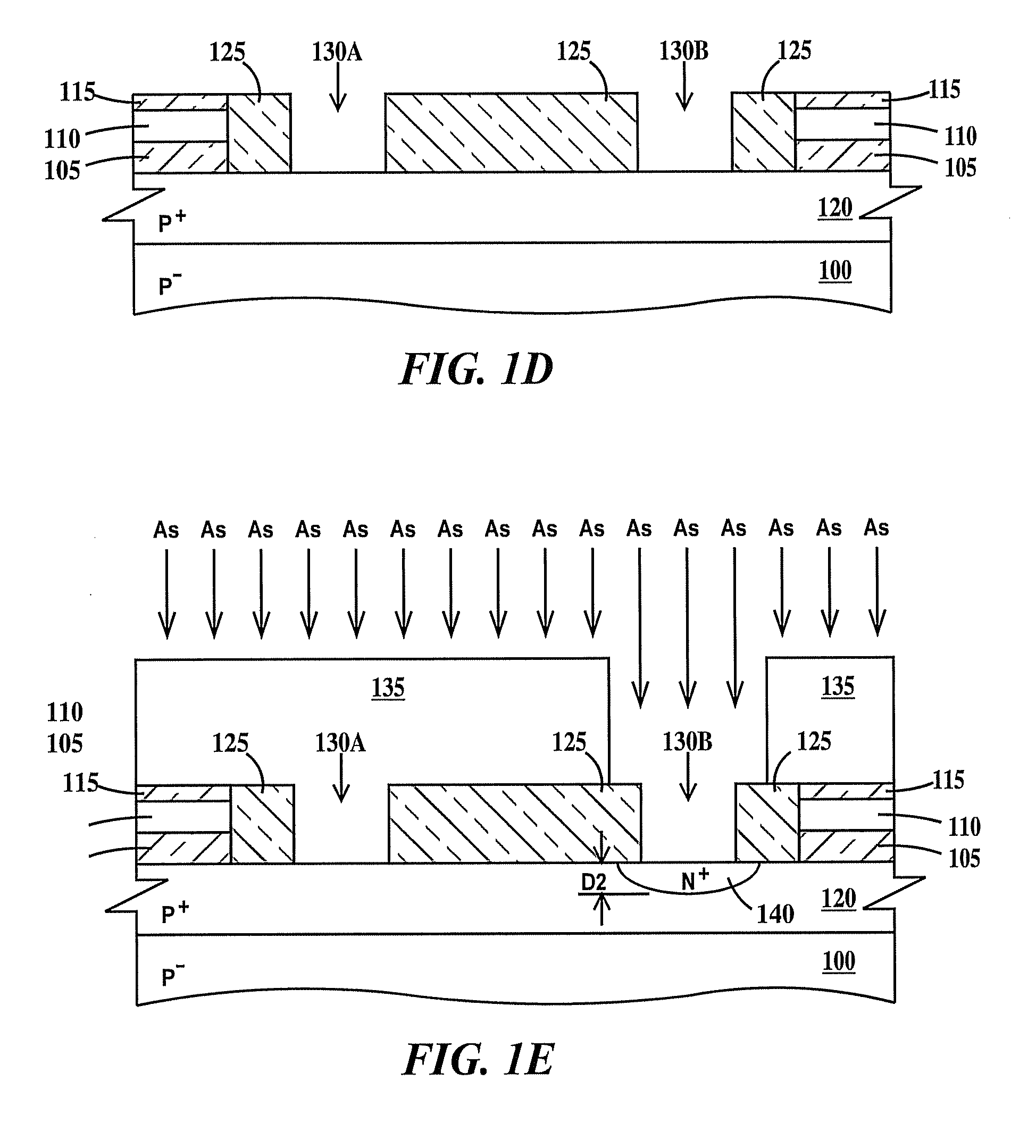
[0017]FIGS. 1A through 1G are cross-sectional drawings illustrating fabrication of an ionizing radiation detection device according to embodiments of the present invention. In FIG. 1A a SOI substrate includes a silicon substrate 100, a buried oxide layer (BOX) 105 on top of silicon substrate 100 and a single-crystal silicon layer 110 on top of BOX 105. A pad oxide layer 115 is formed on top of single-crystal silicon layer 110. In one example, silicon substrate 100 is doped P-type between about 5E15 atm / cm3 and about 5E16 atm / cm3.

[0018]In FIG. 1B a P-type ion-implantation is performed to form doped layer 120. Doped layer 1...


PUM


Abstract

A method, device and system for monitoring ionizing radiation, and design structures for ionizing radiation monitoring devices. The method including: collecting an ionizing radiation induced charge collected by the depletion region of a diode formed in a silicon layer below an oxide layer buried below a surface of a silicon substrate; and coupling a cathode of the diode to a precharged node of a clocked logic circuit such that the ionizing radiation induced charge collected by a depletion region of the diode will discharge the precharged node and change an output state of the clocked logic circuit.

Description

[0001]This application is related to U.S. patent application Ser. No. 11 / 380,736, filed on Apr. 28, 2006.FIELD OF THE INVENTION[0002]The present invention relates to the field of integrated circuits; more specifically, it relates to ionizing radiation monitoring of integrated circuits fabricated on silicon-on-insulator substrates, ionizing radiation monitoring devices and design structure for ionizing radiation monitoring devices.BACKGROUND OF THE INVENTION[0003]The functioning of various integrated circuit devices, such as n-channel field effect transistors (NFETs) and p-channel field effect transistors (PFETs) may be disrupted when the device is struck by ionizing radiation. Disruption of individual devices can lead to failure of the integrated circuit containing the devices. Devices built in silicon-on-insulator (SOI) substrates are particularly sensitive because charge generated by ionizing radiation is difficult to dissipate. Therefore, there is a need to monitor ionizing radia...

Claims


Application Information

Patent Timeline
Patent Type & Authority Applications(United States)
IPC IPC(8): G06F17/50
CPCG11C5/005G11C11/4125H03K19/0033H01L31/115H01L31/118H01L31/103
Inventor ABADEER, WAGDI WILLIAMCANNON, ETHAN HARRISONCOX, DENNIS THOMASTONTI, WILLIAM ROBERT
Owner GLOBALFOUNDRIES INC
Why Eureka
Try Eureka