

Packaging substrate having pattern-matched metal layers
- Summary
- Abstract
- Description
- Claims
- Application Information
AI Technical Summary
Benefits of technology
Problems solved by technology
Method used
Image

Examples
Embodiment Construction
[0084]As stated above, the present invention relates to packaging substrates having pattern-matched metal layers, methods of manufacturing the same, and methods of generating matched patterns for metal layers for the same, which are now described in detail with accompanying figures.
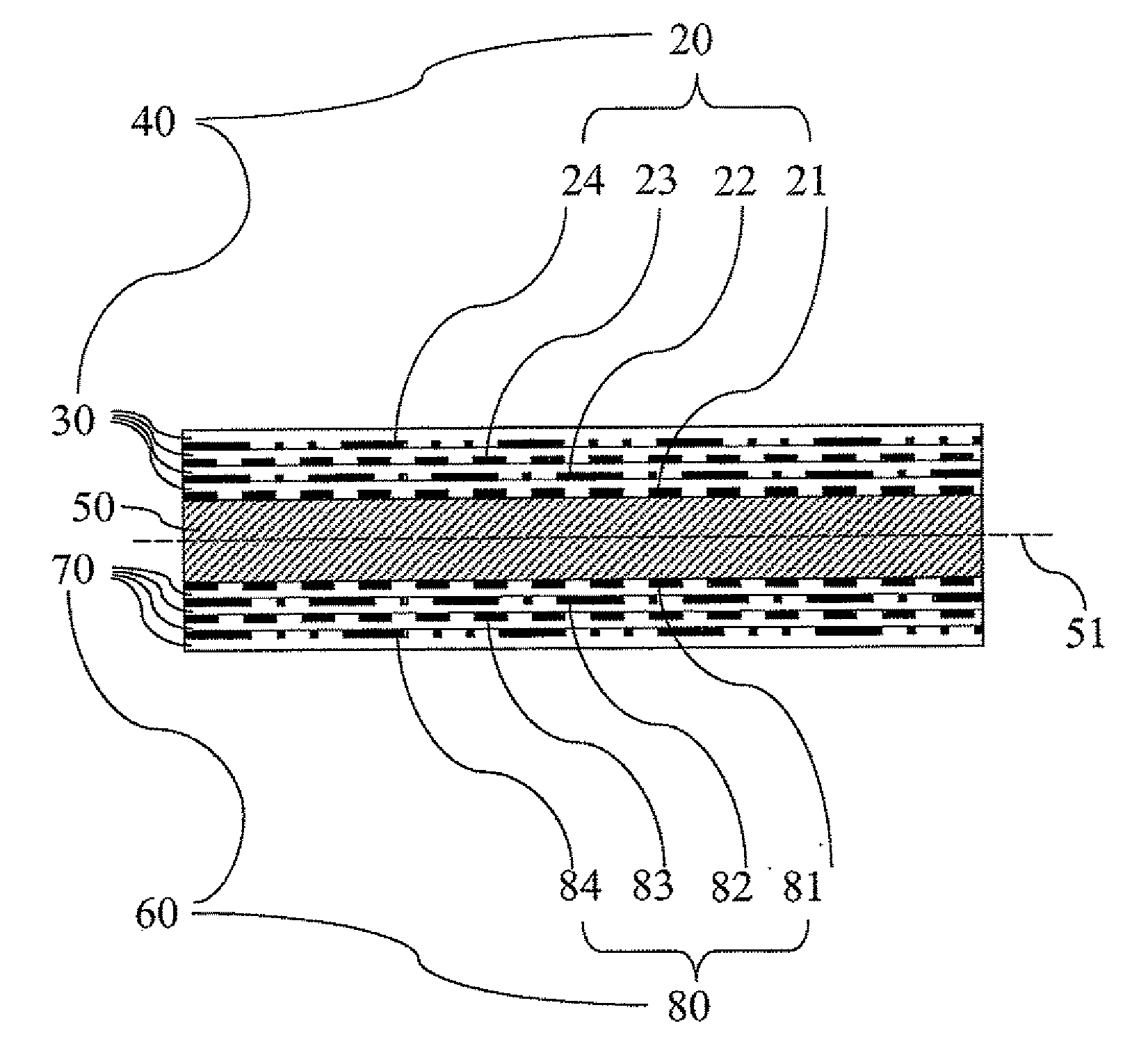
[0085]Referring to FIG. 6, an exemplary packaging substrate according to the present invention comprises a core 50 comprising an insulator material such as a ceramic material or an organic material. The organic material may be reinforced with fiberglass. Also, the organic material may comprise a resin material. In case the insulator material of the core 50 comprises a ceramic material, the exemplary packaging substrate is a ceramic packaging substrate. In case the insulator material of the core 50 comprises an organic material, the exemplary packaging substrate is an organic packaging substrate. While the degree of beneficial effects of the present invention may be greater on an organic packaging substrat...
PUM
| Property | Measurement | Unit |
|---|---|---|
| Fraction | aaaaa | aaaaa |
| Fraction | aaaaa | aaaaa |
| Fraction | aaaaa | aaaaa |
Abstract
Description
Claims
Application Information