Particle-Optical Component

a technology of optical components and parts, applied in the field of particle-optical components, can solve the problems of increasing the complexity of the manufacturing process, the inability to dynamically adjust the capacity for correction of imaging errors in any suitable manner, and the range of new challenges

Active Publication Date: 2009-05-07
APPL MATERIALS ISRAEL LTD +1
View PDF38 Cites 158 Cited by
  • Summary
  • Abstract
  • Description
  • Claims
  • Application Information

AI Technical Summary

Benefits of technology

[0019]It is a still further object of the present invention to provide particle-optical components that allow adjusting a numerical aperture of charged particle beamlets. It is another object of the present invention to provide a particle-optical component that enables testing of a position or other properties of a multi aperture plate and / or optical properties of other optical components of a particle-optical system.

Problems solved by technology

However, the use of multiple beamlets brings about a whole range of new challenges to the design of electron-optical components, arrangements and inspection and processing systems such as microscopes and lithography systems.
Although good results can be achieved with the above-described multi-aperture plates, the above described approaches to correct imaging errors of the particle-optical system require multi-aperture plates having apertures that vary in at least one of shape and size and pattern, or having a resistor network, which is often associated with an increase of a complexity of the manufacturing process.
In addition, the capacity for correction of imaging errors can typically not be dynamically adjusted in any suitable manner when an imaging error of a particle-optical system changes or the component would need transferring to a different system having different properties.

Method used


Image

  • Particle-Optical Component
  • Particle-Optical Component
  • Particle-Optical Component

Examples


Embodiment Construction

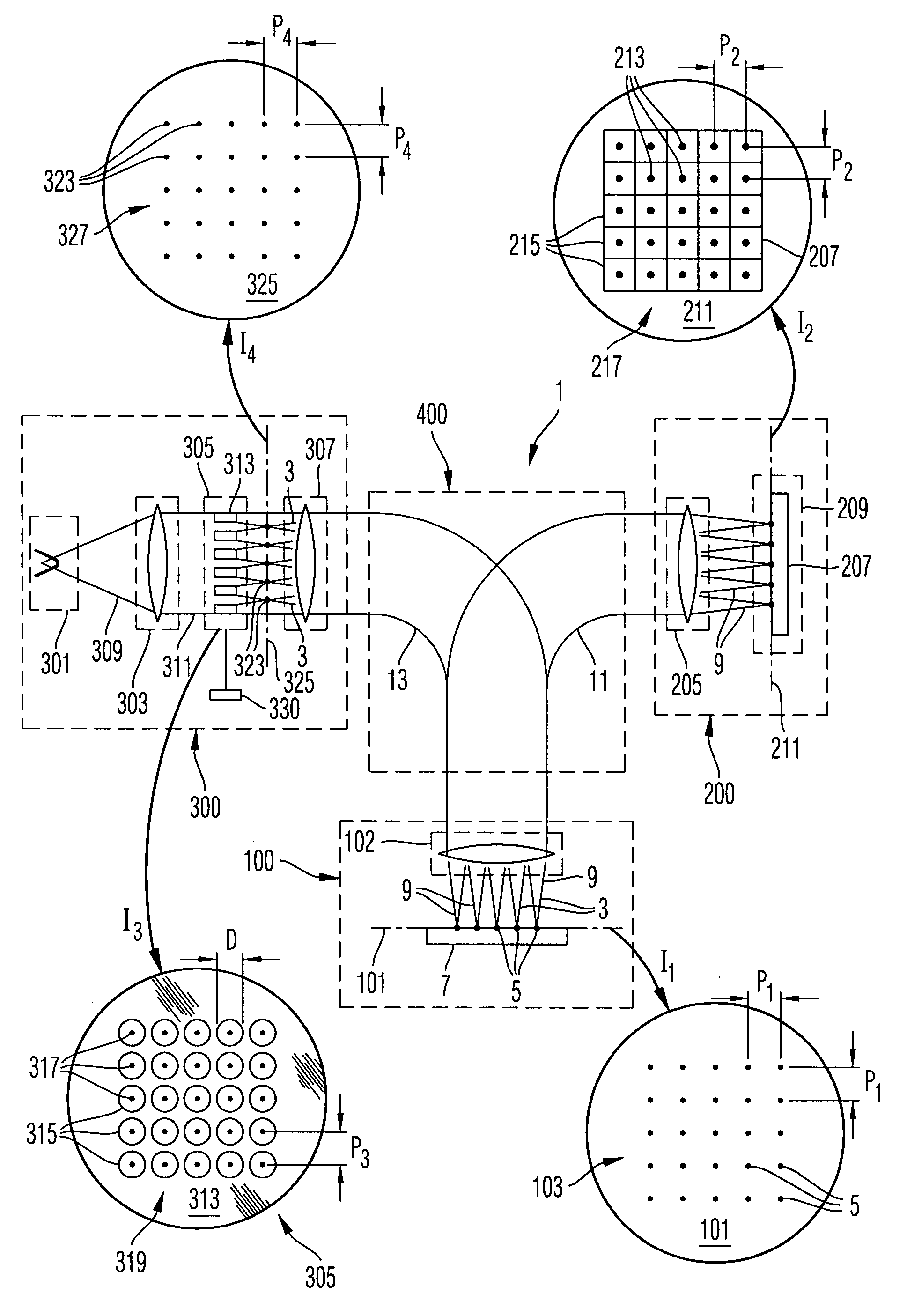
[0209]FIG. 1 is a schematic diagram symbolically illustrating basic functions and features of an electron microscopy system 1 as an embodiment of a particle-optical arrangement, a particle-optical system and an electron multi-beam inspection system as well as a method of manipulating charged particle beamlets according to the present invention. The electron microscopy system 1 is of a scanning electron microscope type (SEM) using a plurality of primary electron beamlets 3 for generating primary electron beam spots 5 on a surface of a specimen 7 to be inspected which surface is arranged in an image plane 101 of an objective lens 102 of an objective arrangement 100.

[0210]Primary electron beamlets 3 are generated by a beamlet generating arrangement 300 comprising an electron source arrangement 301, a collimating lens 303, a particle-optical component 305, illustrated in a simplified form with only one of the two multi-apertures depicted, and a field lens 307.

[0211]The electron source a...


PUM

PropertyMeasurementUnit
diameteraaaaaaaaaa
distanceaaaaaaaaaa
electric potentialsaaaaaaaaaa

Abstract

The present invention relates to a particle-optical component comprising a first multi-aperture plate, and a second multi-aperture plate forming a gap between them; wherein a plurality of apertures of the first multi-aperture plate is arranged such that each aperture of the plurality of apertures of the first multi-aperture plate is aligned with a corresponding aperture of a plurality of apertures of the second multi-aperture plate; and wherein the gap has a first width at a first location and a second width at a second location and wherein the second width is by at least 5% greater than the first width. In addition, the present invention pertains to charged particle systems and arrangements comprising such components and methods of manufacturing multi aperture plates having a curved surface.

Description

BACKGROUND OF THE INVENTION[0001]1. Field of the Invention[0002]The invention relates to particle-optical components for manipulating a plurality of beamlets and particle-optical arrangements and electron-beam inspection systems comprising such particle-optical components. Further, the invention relates to a method of manipulating charged particle beamlets, a method of focusing a plurality of charged particle beamlets and methods for manufacturing multi-aperture plates suitable for use in the particle-optical components. In addition, the invention pertains to a charged-particle multi-beamlet lithography system and a method of writing a pattern on a substrate.[0003]The invention may be applied to charged particles of any type, such as electrons, positrons, muons, ions (charged atoms or molecules) and others.[0004]2. Brief Description of Related Art[0005]The increasing demand for ever smaller and more complex microstructured devices and the continuing demand for an increase of a throu...

Claims


Application Information

Patent Timeline
Patent Type & Authority Applications(United States)
IPC IPC(8): G01N23/00
CPCH01J37/045H01J37/09H01J2237/0435H01J2237/0453H01J2237/15H01J2237/2561H01J2237/2817H01J2237/31774H01J37/3177H01J2237/2446H01J37/04H01J37/145H01J37/147H01J37/244H01J2237/04922H01J2237/04924H01J2237/04926H01J2237/2448
Inventor CASARES, ANTONIOKNIPPELMEYER, RAINERKEMEN, THOMASBAYER, THOMASFRITZ, GEORGGRESCHNER, JOHANNKALT, SAMUEL
Owner APPL MATERIALS ISRAEL LTD
Why Eureka
Try Eureka