Semiconductor device

a technology of semiconductor devices and semiconductors, applied in semiconductor devices, semiconductor/solid-state device details, inductances, etc., can solve the problems of increasing space occupied, difficult to further enhance the q factor of conventional semiconductor devices, and becoming an obstacle to the miniaturization of semiconductor devices, so as to reduce the resistance of inductor, and enhance the q factor

Inactive Publication Date: 2009-05-07
RENESAS ELECTRONICS CORP
View PDF10 Cites 5 Cited by
  • Summary
  • Abstract
  • Description
  • Claims
  • Application Information

AI Technical Summary

Benefits of technology

[0012]Since the inductor and interconnects other than the inductor are formed by an electrolytic plating process in the conventional semiconductor devices, the average grain size of the inductor of conventional semiconductor devices is equivalent to the average grain size of the interconnect in the interconnect layer containing no inductor. On the contrary, in the present invention, the average grain size of an inductor is larger than the average grain size of the interconnect in the copper interconnect layer containing no inductor. Thus, the average grain size of the inductor is larger, as compared with that of the conventional semiconductor device, and reduced resistance of the inductor can be achieved as compared with the conventional semiconductor devices, thereby providing an enhanced Q factor. In the present invention, reduction of the resistance of the inductor is intended by providing an increased average grain size of the inductor. Thus, larger space is not necessary for the inductor, which does not cause an obstacle for miniaturization of the semiconductor device. In the present invention, each of the grain sizes of the respective grains is obtained by an average of the long axis and the short axis of the grain, and the average grain size is number average of the grain sizes. The grain size or the size of the grain may be determined by observing the grain via transmission electron microscopy (TEM). In addition, in the present invention, when an interconnect includes a seed film and a copper film provided over such seed film, the grain size means a grain size of such copper film except the seed film.
[0013]According to the present invention, a semiconductor device, which can achieve an enhanced Q factor of the inductor and can also meet a requirement of a miniaturization of the semiconductor device, is presented.

Problems solved by technology

Further improvement in the Q factor is required in recent years, it is difficult to further enhance the Q factor in the conventional semiconductor devices.
On the other hand, while it is also considered that the linewidth of the inductor is increased for the purpose of providing an increased Q factor of the inductor, such configuration causes an increased space occupied by the inductor in two-dimensional view of the semiconductor device, becoming an obstacle for the miniaturization of the semiconductor device.

Method used


Image

  • Semiconductor device
  • Semiconductor device
  • Semiconductor device

Examples


examples

[0042]Examples of the present invention will be described below.

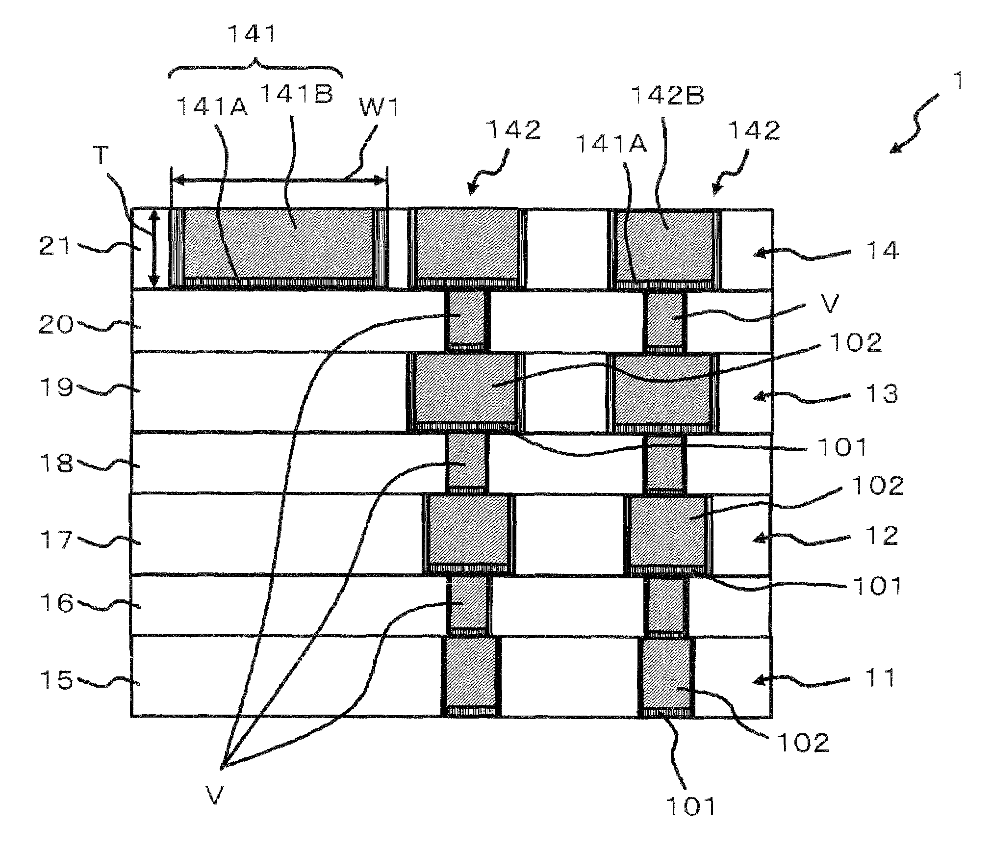
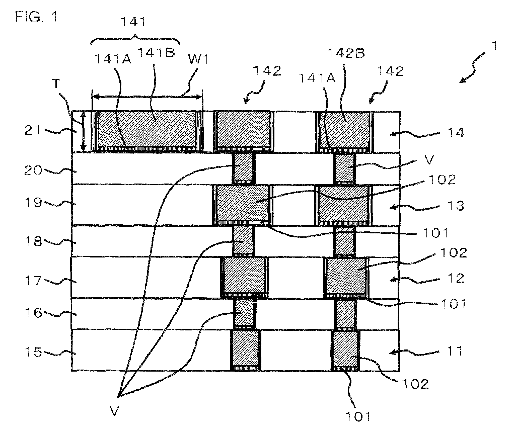
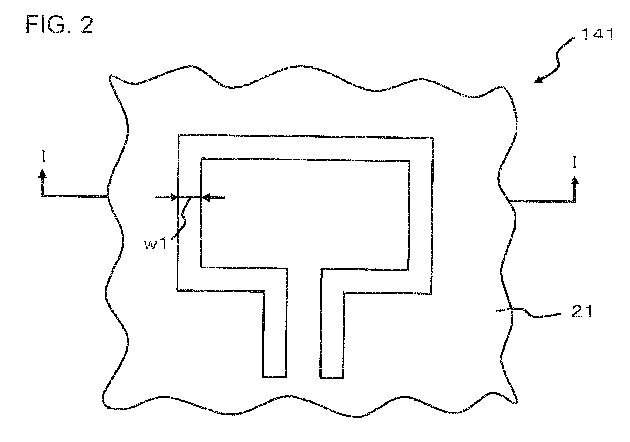
[0043]The semiconductor device 1 was manufactured by a process similar as employed in the above-described embodiment. More specifically, the insulating layer 15 was deposited on the semiconductor substrate, and the interconnect layer 11 of copper was formed in such insulating layer 15. The linewidth of the interconnect layer 11 was 0.1 μm, and the seed film 101 was deposited by a sputtering process. The thickness of such seed film 101 was 100 nm. The copper film 102 was deposited by an electrolytic plating process. Similar operations were repeated to provide the insulating layers 16 to 21 and form interconnect layers 12 and 13 and the vias V. The interconnect layers 12 and 13 and the seed films 101 in the vias V were deposited via a sputtering process. The thickness of the seed films 101 was 100 nm. The copper films 102 were deposited via an electrolytic plating process. In addition to above, silicon carbonitride (SiCN)...


PUM

PropertyMeasurementUnit
grain sizeaaaaaaaaaa
thicknessaaaaaaaaaa
grain sizeaaaaaaaaaa

Abstract

A semiconductor device 1 includes: a copper interconnect layer 14 that has an interconnect containing an inductor 141, which is buried in an interconnect trench formed in an insulating layer 21; and copper interconnect layers 11 to 13, which include no inductor and are buried in interconnect trenches formed in other insulating layers 15, 17 and 19, respectively. An average grain size of the inductor 141 is larger than average grain sizes of the interconnects in the copper interconnect layers 11 to 13 that contain no inductor

Description

[0001]This application is based on Japanese patent application No. 2007-288,291, the content of which is incorporated hereinto by reference.BACKGROUND[0002]1. Technical Field[0003]The present invention relates to a semiconductor device.[0004]2. Related Art[0005]Conventionally, as shown in FIGS. 6 and 7, an inductor 901 is provided in a semiconductor device 900 (see Japanese Patent Laid-Open No. 2004-31,520). FIG. 7 is a cross-sectional view along line VII-VII of FIG. 6. Such inductor 901 is provided in an interconnect layer 904 of an uppermost layer of a multiple-layered interconnect, and is disposed on the insulating layer 903. An insulating layer 905 and an insulating layer 902, which are composed of silicon dioxide (SiO2), are provided on the inductor 901. Since the inductor 901 is provided on the uppermost interconnect layer 904, a parasitic capacitance between the semiconductor substrate and the inductor 901 is reduced, and the thickness of the inductor 901 is increased to redu...

Claims


Application Information

Patent Timeline
Patent Type & Authority Applications(United States)
IPC IPC(8): H01L29/00
CPCH01L21/2855H01L21/2885H01L21/76877H01L28/10H01L23/5227H01L23/53238H01L21/76883H01L2924/0002H01L2924/00
Inventor NAKASHIBA, YASUTAKATAKEWAKI, TOSHIYUKI
Owner RENESAS ELECTRONICS CORP
Why Eureka
Try Eureka