Hybrid laser diode

a laser diode and hybrid technology, applied in the field of semiconductor lasers, can solve the problems of large leakage current, low thermal stability, and technical limitations of related hybrid laser diodes, and achieve the effects of reducing typical thermal limitations, and reducing the loss of waveguide modes

Inactive Publication Date: 2009-05-07
ELECTRONICS & TELECOMM RES INST
View PDF8 Cites 40 Cited by
  • Summary
  • Abstract
  • Description
  • Claims
  • Application Information

AI Technical Summary

Benefits of technology

[0030]According to the present invention, provided is a hybrid laser diode using a silicon layer and a III-V group semiconductor layer as a slab waveguide and a channel waveguide, respectively. Since the channel waveguide is formed through patterning, a current path for an operation of a light emitting diode is discretely defined. Accordingly, typical limitations such as leakage current, series resistance, and power consumption can be resolved. Moreover, because the slab waveguide directly contacts the entire bottom surface of a light emitting diode, a typical thermal limitation can be also reduced.
[0031]Furthermore, according to the present invention, because a silicon layer where most of a waveguide mode is distributed is used as a slab waveguide, the loss of a waveguide mode due to its change can be reduced. Moreover, a coupling structure connecting the slab waveguide with a predetermined optical device contributes to reducing the loss of the waveguide mode. As a result, a hybrid laser diode according to the present invention can have a high coupling efficiency.

Problems solved by technology

On the other hand, a related hybrid laser diode has technical limitations such as large leakage current, low thermal stability, and high series resistance.
Furthermore, as described above, the void region 99 filled with air has a low thermal conductivity, and thus heat generated from the light emitting diode 42 may not be efficiently emitted.
Since operational and optical characteristics of a laser diode are very susceptible to a temperature, these poor thermal emission characteristics may deteriorate product characteristics.

Method used


Image

  • Hybrid laser diode
  • Hybrid laser diode
  • Hybrid laser diode

Examples


Embodiment Construction

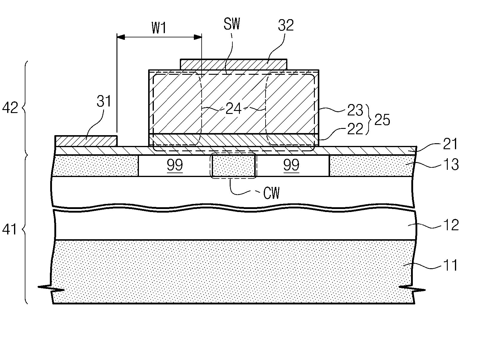
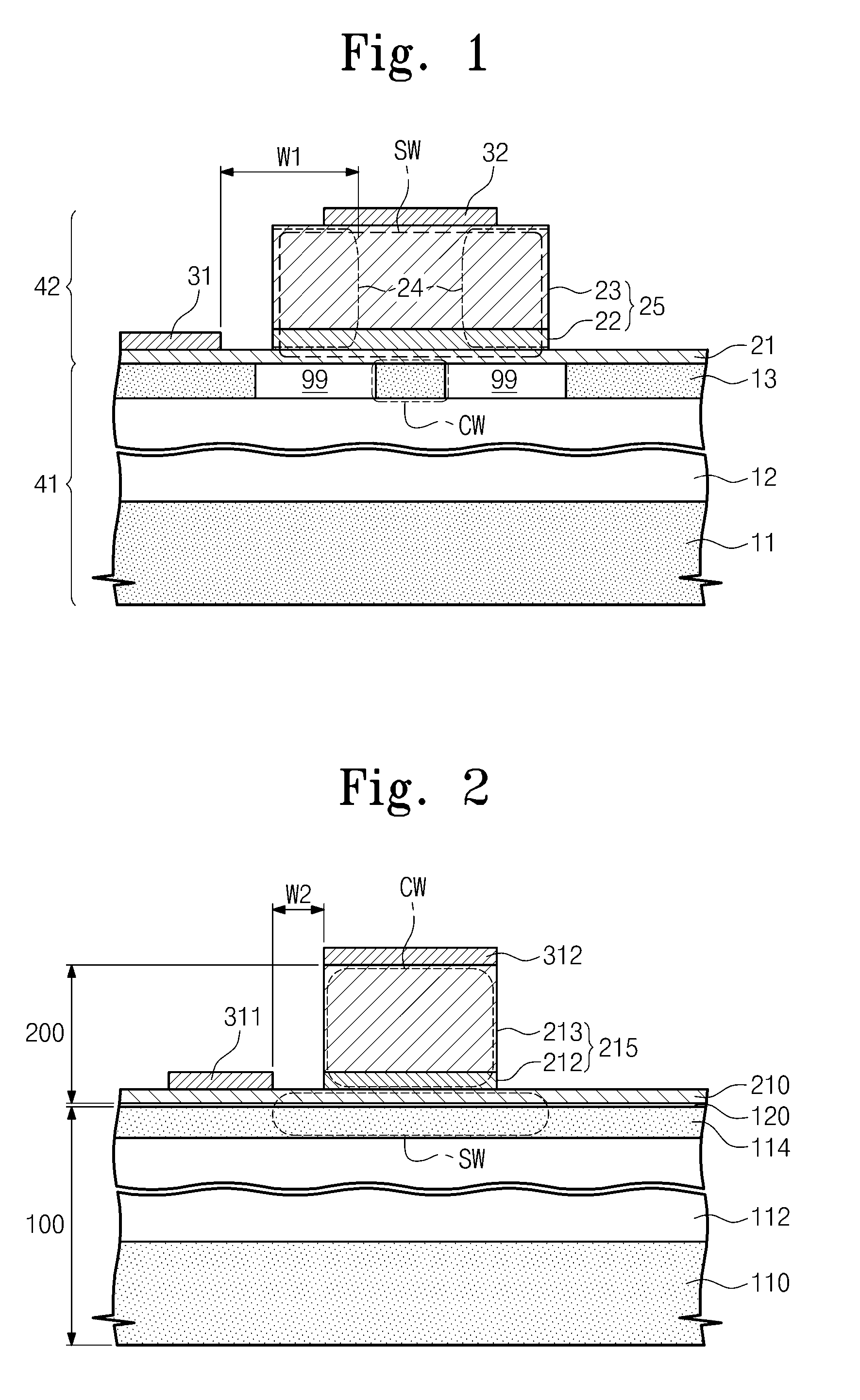
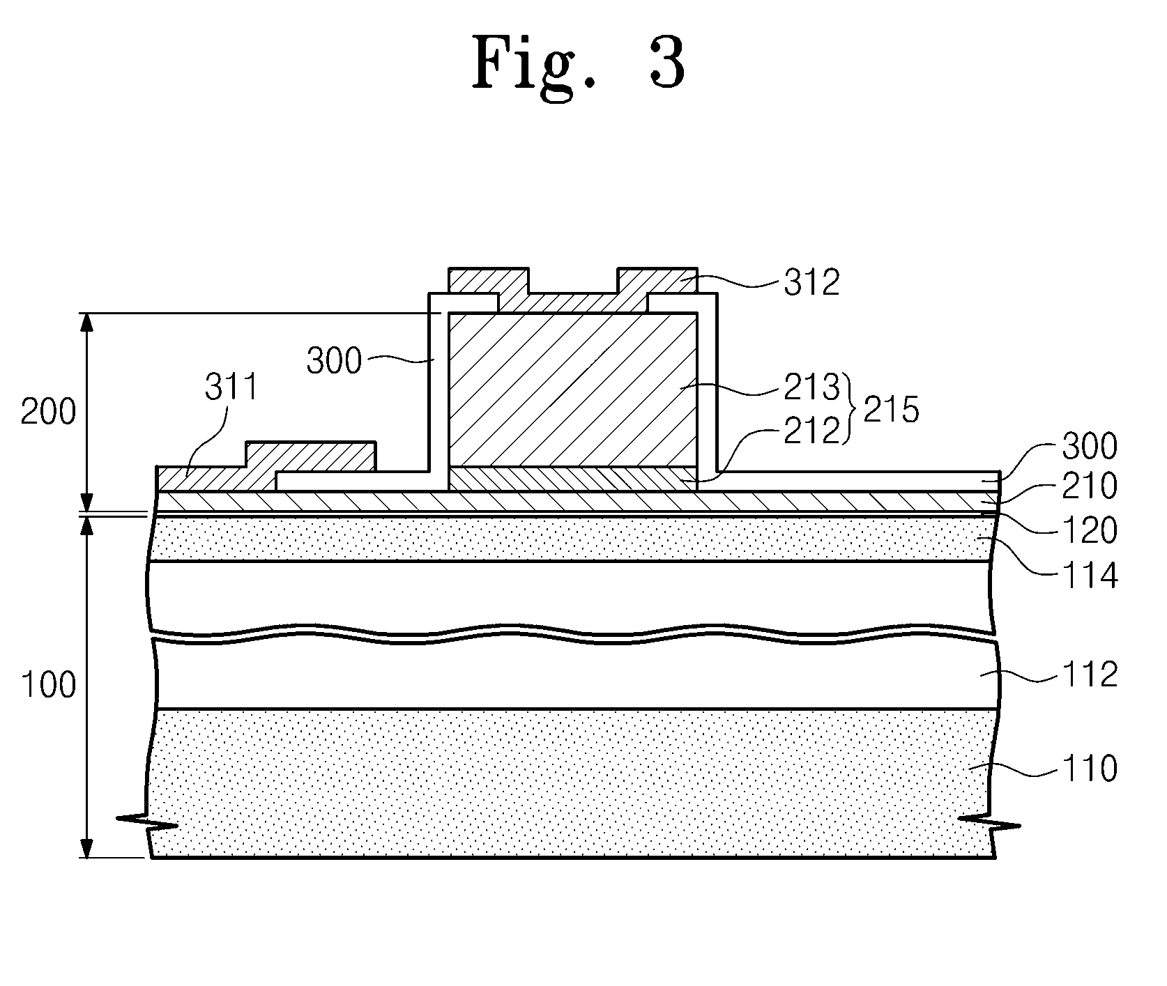
[0045]Preferred embodiments of the present invention will be described below in more detail with reference to the accompanying drawings. The present invention may, however, be embodied in different forms and should not be construed as limited to the embodiments set forth herein. Rather, these embodiments are provided so that this disclosure will be thorough and complete, and will fully convey the scope of the present invention to those skilled in the art.

[0046]In the figures, the dimensions of layers and regions are exaggerated for clarity of illustration. It will also be understood that when a layer (or film) is referred to as being ‘on’ another layer or substrate, it can be directly on the other layer or substrate, or intervening layers may also be present. Further, it will be understood that when a layer is referred to as being ‘under’ another layer, it can be directly under, and one or more intervening layers may also be present. In addition, it will also be understood that when...


PUM


Abstract

Provided is a hybrid laser diode. The hybrid laser diode includes: a silicon layer constituting a slab waveguide; and a compound semiconductor layer disposed on the silicon layer to constitute a channel waveguide.

Description

CROSS-REFERENCE TO RELATED APPLICATIONS[0001]This U.S. non-provisional patent application claims priority under 35 U.S.C. § 119 of Korean Patent Application No. 10-2007-113130, filed on Nov. 7, 2007, the entire contents of which are hereby incorporated by reference.BACKGROUND OF THE INVENTION[0002]The present invention disclosed herein relates to a semiconductor device, and more particularly, to a hybrid laser diode.[0003]The present invention has been derived from research undertaken as a part of the information technology (IT) development business by the Ministry of Information and Communication and the Institute for Information Technology Advancement of the Republic of Korea [Project management No.: 2006-S-004-02, Project title: silicon-based high speed optical interconnection IC].[0004]A hybrid laser diode using silicon and a III-V group compound semiconductor receives attention as a light source for photonics technology combining optical technology with electronic device techno...

Claims


Application Information

Patent Timeline
Patent Type & Authority Applications(United States)
IPC IPC(8): H01S5/00
CPCG02B6/12004G02B2006/12121G02B2006/12152H01S5/021H01S5/0215H01S5/32333H01S5/026H01S5/1014H01S5/1032H01S5/32316H01S5/0218B82Y40/00H01S3/0941
Inventor LEEM, YOUNG-AHNSONG, JUNG-HOKIM, KI-SOOKWON, O-KYUNKIM, GYUNG-OCK
Owner ELECTRONICS & TELECOMM RES INST
Why Eureka
Try Eureka