MEMS diaphragm structure and method for forming the same

a diaphragm and diaphragm technology, applied in the field of acceleration sensors and pressure sensors, can solve the problems of difficult to freely vary and the amplitude of the diaphragm cannot be freely varied, so as to improve the resistance of the diaphragm against film breakage, easy to form, and easy to rounded

Inactive Publication Date: 2009-05-07
PANASONIC CORP
View PDF4 Cites 46 Cited by
  • Summary
  • Abstract
  • Description
  • Claims
  • Application Information

AI Technical Summary

Benefits of technology

[0018]In view of the problem mentioned above, an object of the present invention is to provide a diaphragm having a hinge structure in which the stress concentration on hinge corner portions is prevented to improve reliability of the diaphragm.Means for Solving the Problems
[0058]Moreover, according to the invention, by using a method in which a sidewall spacer is formed on a hinge pattern side wall, the film thickness of a hinge corner portion of the diaphragm can be easily increased for reinforcement, and the hinge corner portion can be easily formed to have an obtuse angle or rounded. Moreover, since the bending angle and the round shape of the hinge corner portion can be controlled by controlling steps for forming the sidewall spacer, the stress concentration on the hinge corner portion can be dispersed to improve the resistance of the diaphragm against film breakage. That is, the present invention can realize a structure of a diaphragm having an excellent hinge structure and a method for forming the same.

Problems solved by technology

However, in this method, the film type, the film thickness, or the like is often restricted by a diaphragm formation process, and thus it is difficult to freely vary the amplitude of the diaphragm.
However, also in this method, since the chip size is restricted by a final product form, the amplitude of the diaphragm can not be freely varied.

Method used


Image

  • MEMS diaphragm structure and method for forming the same
  • MEMS diaphragm structure and method for forming the same
  • MEMS diaphragm structure and method for forming the same

Examples


embodiment 1

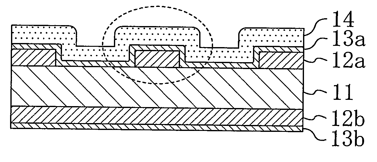
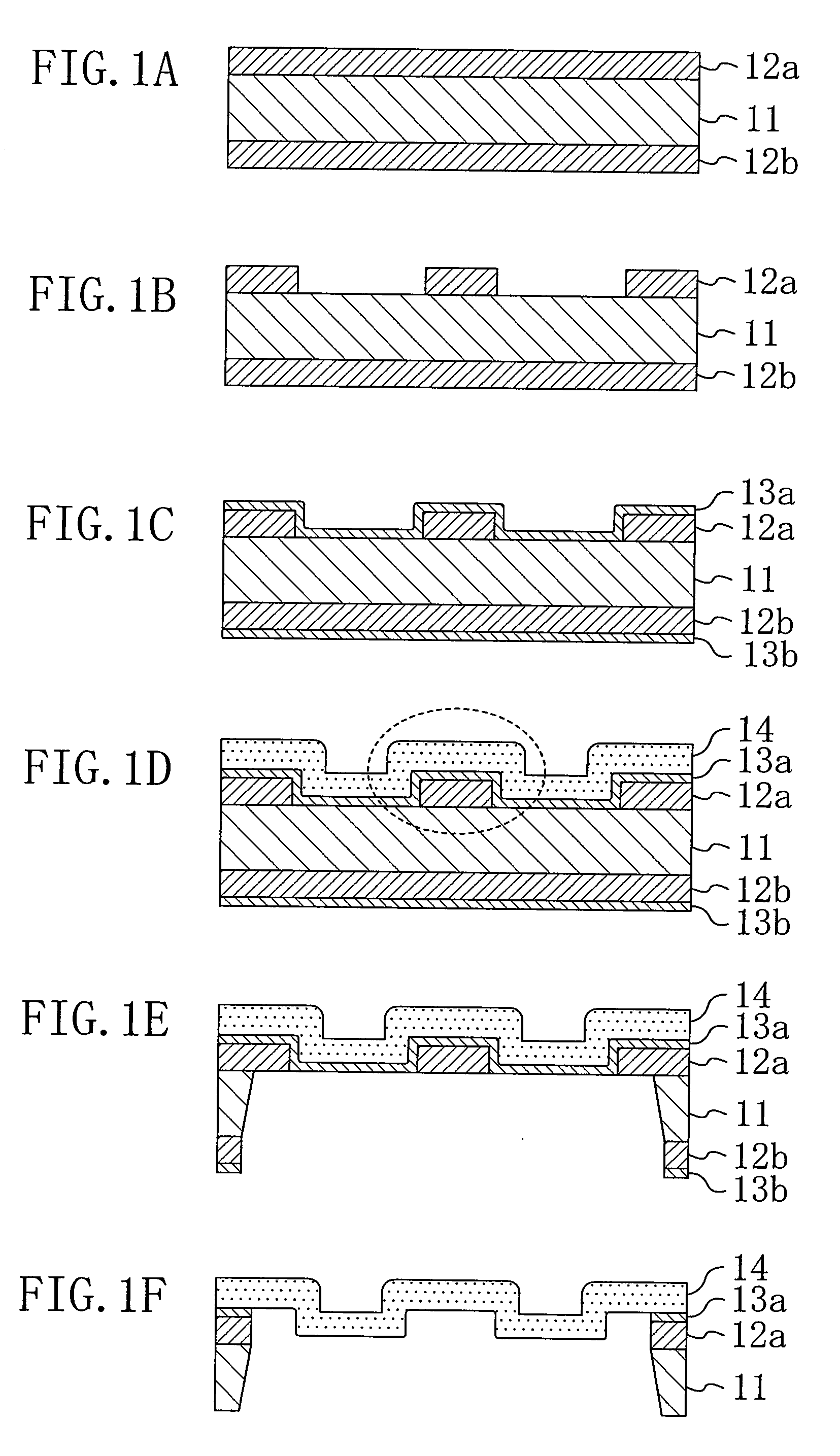
[0091]A MEMS diaphragm structure having a hinge and a method for forming the same according to Embodiment 1 of the present invention will be described below with reference to the drawings.

[0092]FIGS. 1A through 1F are cross-sectional views illustrating respective steps of the method for forming the diaphragm structure of Embodiment 1.

[0093]First, as illustrated with FIG. 1A, a first film 12a is formed on an upper surface of a silicon substrate 11. Here, the first film 12a desirably has a thickness of greater than or equal to about 100 nm, because the thickness of the first film 12a is a parameter which determines the height (level difference between the highest position and the lowest position in the diaphragm) of a hinge structure of a diaphragm which is to be finally formed. Moreover, since the first film 12a is finally removed by etching, the first film 12a is desirably a silicon oxide film. A silicon oxide film can be formed by thermal oxidation, low pressure CVD, plasma CVD, or...

embodiment 2

[0102]A MEMS diaphragm structure having a hinge and a method for forming the same according to Embodiment 2 of the present invention will be described below with reference to the drawings.

[0103]FIGS. 3A through 3H are cross-sectional views illustrating respective steps of the method for forming the diaphragm structure of Embodiment 2.

[0104]First, as illustrated with FIG. 3A, a first film 22a is formed on an upper surface of a silicon substrate 21. Here, the first film 22a desirably has a thickness of greater than or equal to about 100 nm, because the thickness of the first film 22a is a parameter which determines the height of a hinge structure of a diaphragm which is to be finally formed. Moreover, since the first film 22a is finally removed by etching, the first film 22a is desirably a silicon oxide film. A silicon oxide film can be formed by thermal oxidation, low pressure CVD, plasma CVD, or the like. In the case of using thermal oxidation or low pressure CVD, a silicon oxide fi...

embodiment 3

[0117]A MEMS diaphragm structure having a hinge and a method for forming the same according to Embodiment 3 of the present invention will be described below with reference to the drawings.

[0118]FIGS. 5A through 5H are cross-sectional views illustrating respective steps of the method for forming the diaphragm structure of Embodiment 3.

[0119]First, as illustrated with FIG. 5A, a first film 32a is formed on an upper surface of a silicon substrate 31. Here, the first film 32a desirably has a thickness of greater than or equal to about 100 nm, because the thickness of the first film 32a is a parameter which determines the height of a hinge structure of a diaphragm which is to be finally formed. Moreover, since the first film 32a is finally removed by etching, the first film 32a is desirably a silicon oxide film. A silicon oxide film can be formed by thermal oxidation, low pressure CVD, plasma CVD, or the like. In the case of using thermal oxidation or low pressure CVD, a silicon oxide fi...


PUM


Abstract

A diaphragm (14) is formed using MEMS technology. The diaphragm (14) has a hinge structure, and at least one of a hinge upper corner portion and a hinge lower corner portion of the diaphragm (14) is rounded.

Description

TECHNICAL FIELD[0001]The present invention relates to an acceleration sensor, a pressure sensor, or the like using MEMS (Micro Electro Mechanical Systems) technology. Specifically, the present invention relates to a structure of a diaphragm serving as a part detecting an acceleration change, a pressure change, or the like and then vibrating and to a method for forming the same.BACKGROUND ART[0002]In recent years, advances have been made in a technical field called MEMS by making use of fine processing technology used in a field of fabricating LSI (large-scale integrated) circuits adopting a semiconductor such as silicon. By using the MEMS technology, various types of fine components such as an acceleration sensor and a pressure sensor have been proposed and produced on a commercial basis.[0003]The acceleration sensor or the pressure sensor includes a diaphragm serving as a part detecting an acceleration change or a pressure change and then vibrating.[0004]FIGS. 13A through 13E are c...

Claims


Application Information

Patent Timeline
IPC IPC(8): H04R19/04G01P15/125H01L21/306
CPCB81B3/0072B81B2201/0257H04R19/005G01P15/0802G01P15/125B81B2203/0127G01P2015/084
Inventor MIYOSHI, YUICHI
Owner PANASONIC CORP
Why Eureka
Try Eureka