Photoelectric conversion device and method for manufacturing the same

a technology of photoelectric conversion and conversion device, which is applied in the direction of semiconductor/solid-state device manufacturing, semiconductor devices, electrical apparatus, etc., can solve the problems of limited resources effectively used, difficult to produce enough photoelectric conversion devices to meet the demand, and inability to maintain bond strength for a long time, etc., and achieve the effect of effective resource us

Inactive Publication Date: 2009-05-14
SEMICON ENERGY LAB CO LTD
View PDF39 Cites 43 Cited by
  • Summary
  • Abstract
  • Description
  • Claims
  • Application Information

AI Technical Summary

Benefits of technology

[0013]In accordance with the present invention, a single crystal semiconductor substrate is sliced from the top surface thereof and bonded to a supporting substrate, whereby a photoelectric conversion device in which a top cell is stacked over a bottom cell can be obtained. The bottom cell uses a single crystal semiconductor layer with a thickness of 10 μm or less as a photoelectric conversion layer, and the top cell uses a non-single-crystal semiconductor layer as a photoelectric conversion layer. That is to say, a photoelectric conversion device can be manufactured in which a bottom cell using a single crystal semiconductor layer as a photoelectric conversion layer and a top cell using a non-single-crystal semiconductor layer as a photoelectric conversion layer, which is stacked over the bottom cell, are provided over a large-area glass substrate the upper temperature limit of which is equal to or lower than 700° C. The single crystal semiconductor layer is obtained by separation of an upper portion of the single crystal semiconductor substrate. The single crystal semiconductor substrate which can be repeatedly used enables effective use of resources.

Problems solved by technology

Conventionally, it has been difficult to produce photoelectric conversion devices enough to meet the demand, with limited resources effectively utilized.
Further, in a method for bonding a single crystal semiconductor layer which is formed into a slice to a support substrate with a conductive paste, there is a problem such that bond strength cannot be maintained for a long time.
In particular, in a condition in which a photovoltaic device is exposed to direct sunlight, there is a problem such that an organic material contained in a conductive paste is modified and bond strength is lowered.
In addition, there is a problem of reliability such that a conductive material (e.g., silver) in the conductive paste is diffused into the single crystal semiconductor layer, which deteriorates photoelectric conversion characteristics of a semiconductor.

Method used


Image

  • Photoelectric conversion device and method for manufacturing the same
  • Photoelectric conversion device and method for manufacturing the same
  • Photoelectric conversion device and method for manufacturing the same

Examples


embodiment mode 1

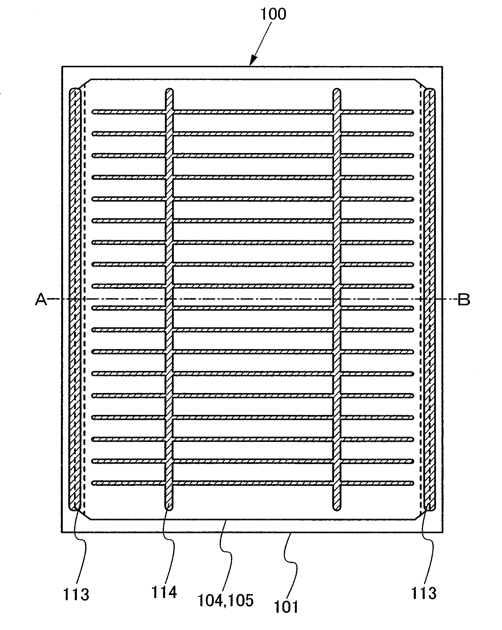
[0033]FIG. 1 is a plan view of a photoelectric conversion device 100 of this embodiment mode. This photoelectric conversion device 100 includes a first unit cell 104 and a second unit cell 105 which are fixed to a supporting substrate 101. The first unit cell 104 and the second unit cell 105 include semiconductor junction by which photoelectric conversion is performed.

[0034]The first unit cell 104 is provided with a first electrode on the supporting substrate 101 side and the second unit cell 105 is provided with a second electrode on the surface side. The first electrode is connected to a first auxiliary electrode 113 and a second auxiliary electrode 114 is provided over the second electrode. The photoelectric conversion device 100 of this embodiment mode has a structure in which the first unit cell 104 and the second unit cell 105 are stacked over the supporting substrate 101 having an insulating surface; therefore, positive and negative electrodes are exposed to the same surface ...

embodiment mode 2

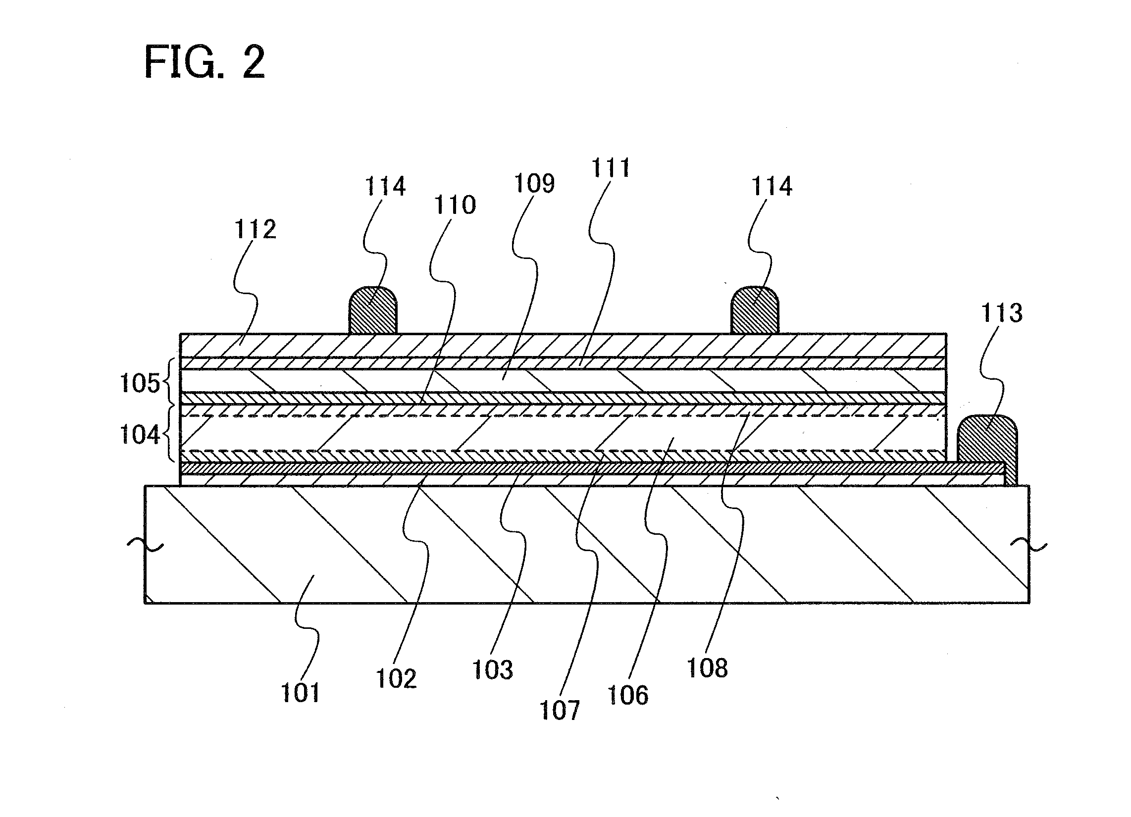
[0050]Next, a method for manufacturing the photoelectric conversion device 100 with its cross-sectional structure along section line A-B of FIG. 1 corresponding to the structure shown in FIG. 2 will be described.

[0051]A semiconductor substrate 119 shown in FIG. 5A is a substrate with a shape about a quadrangular shape, cut out from a circular single crystal semiconductor substrate. The shape of a top surface of the semiconductor substrate 119 is not limited in particular; however, the semiconductor substrate 119 preferably has the shape about a quadrangular shape in the case where a supporting substrate which supports a single crystal semiconductor layer is rectangular in shape. The semiconductor substrate 119 is typically single crystal silicon and preferably has its surface polished to have a mirror surface. This is because the semiconductor substrate 119 is disposed in close contact with the supporting substrate with an insulating layer for bonding interposed therebetween. For ex...

embodiment mode 3

[0083]In Embodiment Mode 2, in some cases, due to the formation of the damaged layer 121, crystal defects remain at the surface of the single crystal semiconductor layer 106 which is exposed through the separation of part of the semiconductor substrate 119 shown in FIG. 6B. In those cases, it is preferable that the surface portion of the single crystal semiconductor layer 106 be removed by etching. For the etching, either dry etching or wet etching is performed. Further, in some cases, a rough surface remains in which mean surface roughness (Ra) is 7 to 10 nm and the largest difference in height between peak and valley (P−V) is 300 to 400 nm. The ‘largest difference in height between peak and valley’ in this specification refers to a difference in height between the peak and valley. The ‘peak’ and the ‘valley’ in this embodiment refer to a peak and a valley obtained by three-dimensional expansion of the “peak” and the “valley” defined by JIS B0101. The peak is represented as the hig...


PUM


Abstract

A photoelectric conversion device with an excellent photoelectric conversion characteristic with a silicon semiconductor material effectively utilized. The photoelectric conversion device includes a first unit cell including a first electrode, a first impurity semiconductor layer, a single crystal semiconductor layer, and a second impurity semiconductor layer; and a second unit cell including a third impurity semiconductor layer, a non-single-crystal semiconductor layer, a fourth impurity semiconductor layer, and a second electrode. The second and third impurity semiconductor layers are in contact with each other so that the first and second unit cells are connected in series, and an insulating layer is provided for a surface of the first electrode and bonded to a supporting substrate.

Description

TECHNICAL FIELD[0001]The present invention relates to a photoelectric conversion device using a single crystal semiconductor or a polycrystalline semiconductor, and relates to a so-called tandem photoelectric conversion device in which a plurality of photoelectric conversion elements are stacked.BACKGROUND ART[0002]As a measure against global warming, solar photovoltaic power generation has become popular in the world. For the solar photovoltaic power generation, a photoelectric conversion device (also called a solar cell) in which light energy is converted into electrical energy by using photoelectric characteristics of a semiconductor is applied in many cases, as compared to the case of utilizing solar heat.[0003]Production of photoelectric conversion devices tends to increase year after year. For example, the total production of solar cells in the world in 2005 was 1,759 MW, which is a drastic increase of 147% as compared to that in the previous fiscal year. Photoelectric convers...

Claims


Application Information

Patent Timeline
Patent Type & Authority Applications(United States)
IPC IPC(8): H01L31/18H01L31/0376
CPCH01L31/076Y02E10/548H01L31/18
Inventor YAMAZAKI, SHUNPEIARAI, YASUYUKI
Owner SEMICON ENERGY LAB CO LTD
Why Eureka
Try Eureka